Simplified Method of Producing an Epitaxially Grown Structure

a technology of epitaxial growth and simplified method, which is applied in the direction of crystal growth process, basic electric elements, electrical equipment, etc., can solve the problem that no satisfactory method is known to produce said growth seeds

Inactive Publication Date: 2008-11-06
COMMISSARIAT A LENERGIE ATOMIQUE ET AUX ENERGIES ALTERNATIVES
View PDF7 Cites 38 Cited by
  • Summary
  • Abstract
  • Description
  • Claims
  • Application Information

AI Technical Summary

Problems solved by technology

The problems generated by this method are that it requires a lithography step to etch the mask or the crystalline layer, and thereby define growth seeds.
At the present time no satisfactory method is known to produce said growth seeds in collective, orderly fashion on the scale of a substrate whose diameter may reach 300 millimeters and over.

Method used


Image

  • Simplified Method of Producing an Epitaxially Grown Structure
  • Simplified Method of Producing an Epitaxially Grown Structure
  • Simplified Method of Producing an Epitaxially Grown Structure

Examples


Embodiment Construction

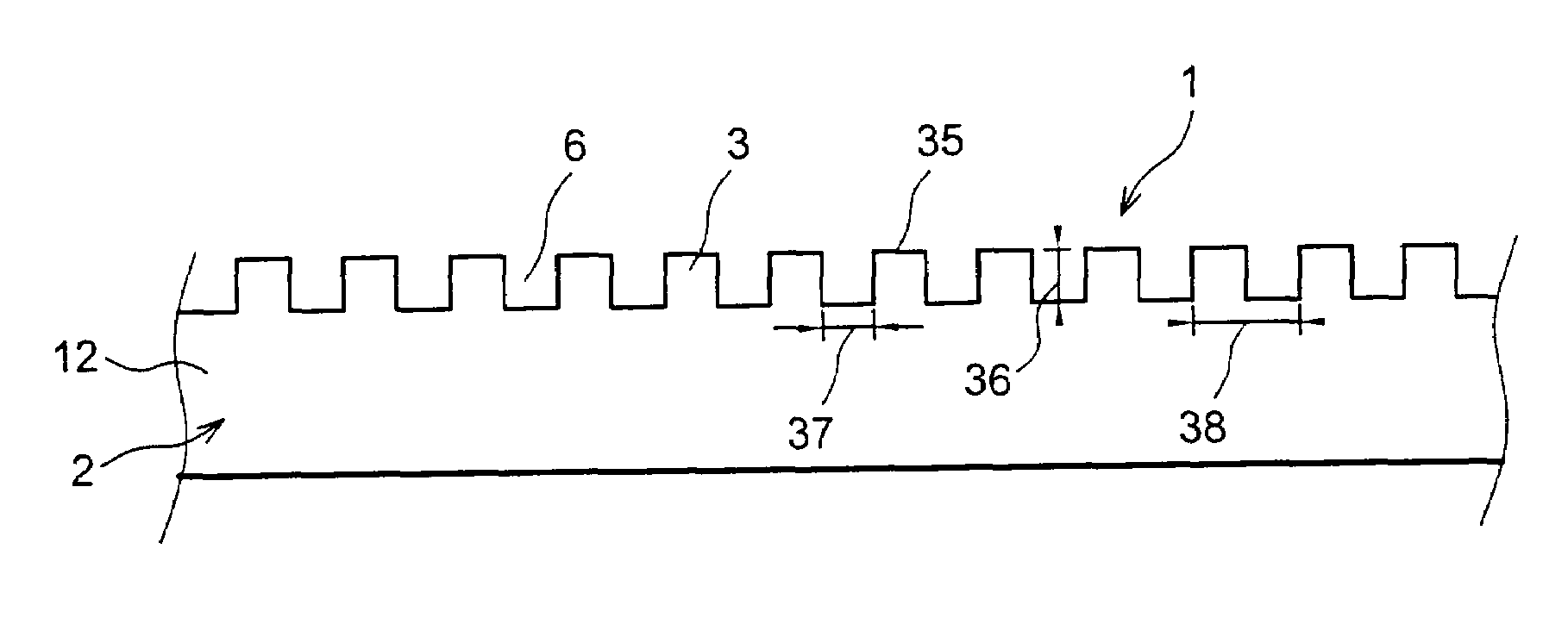
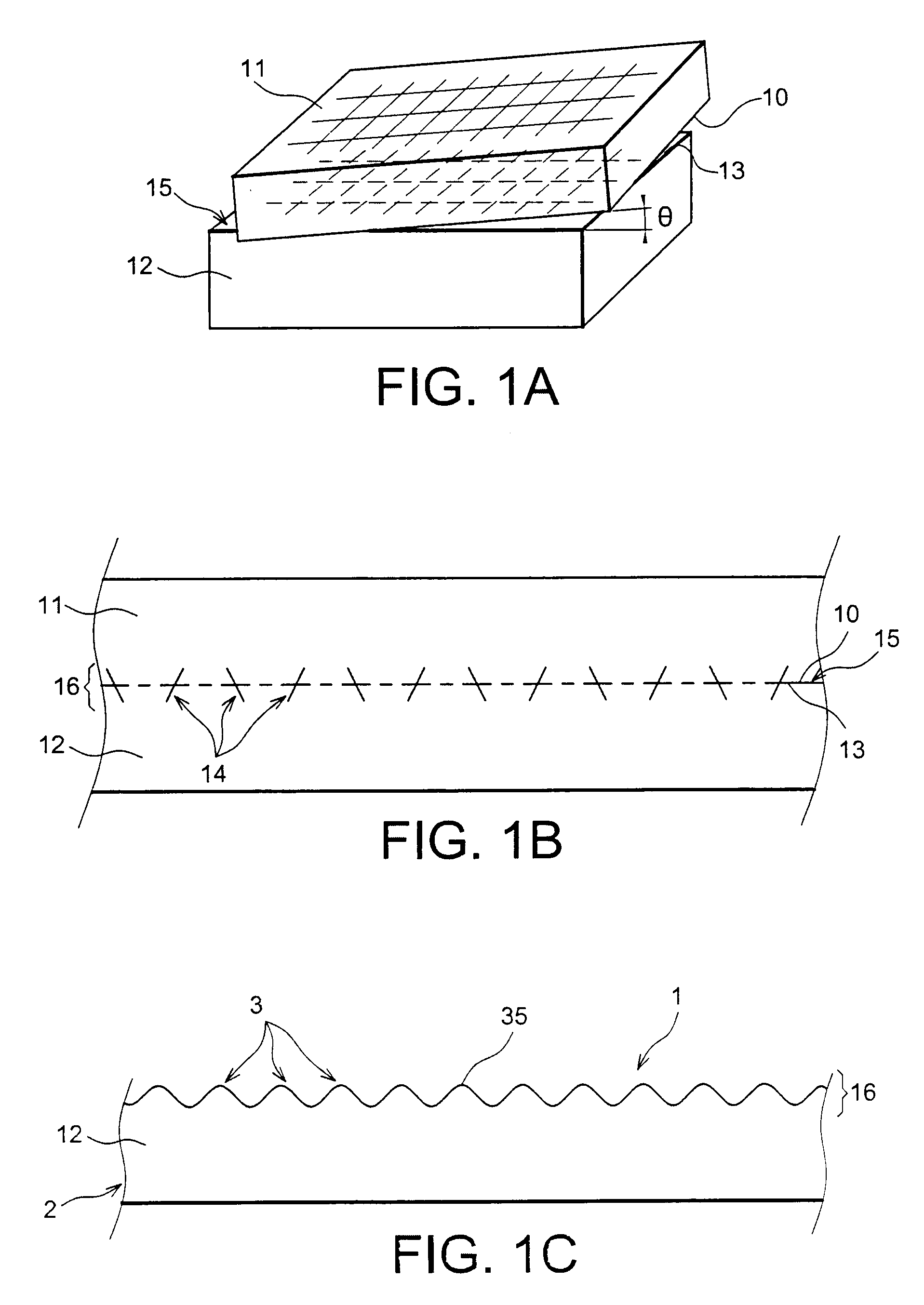
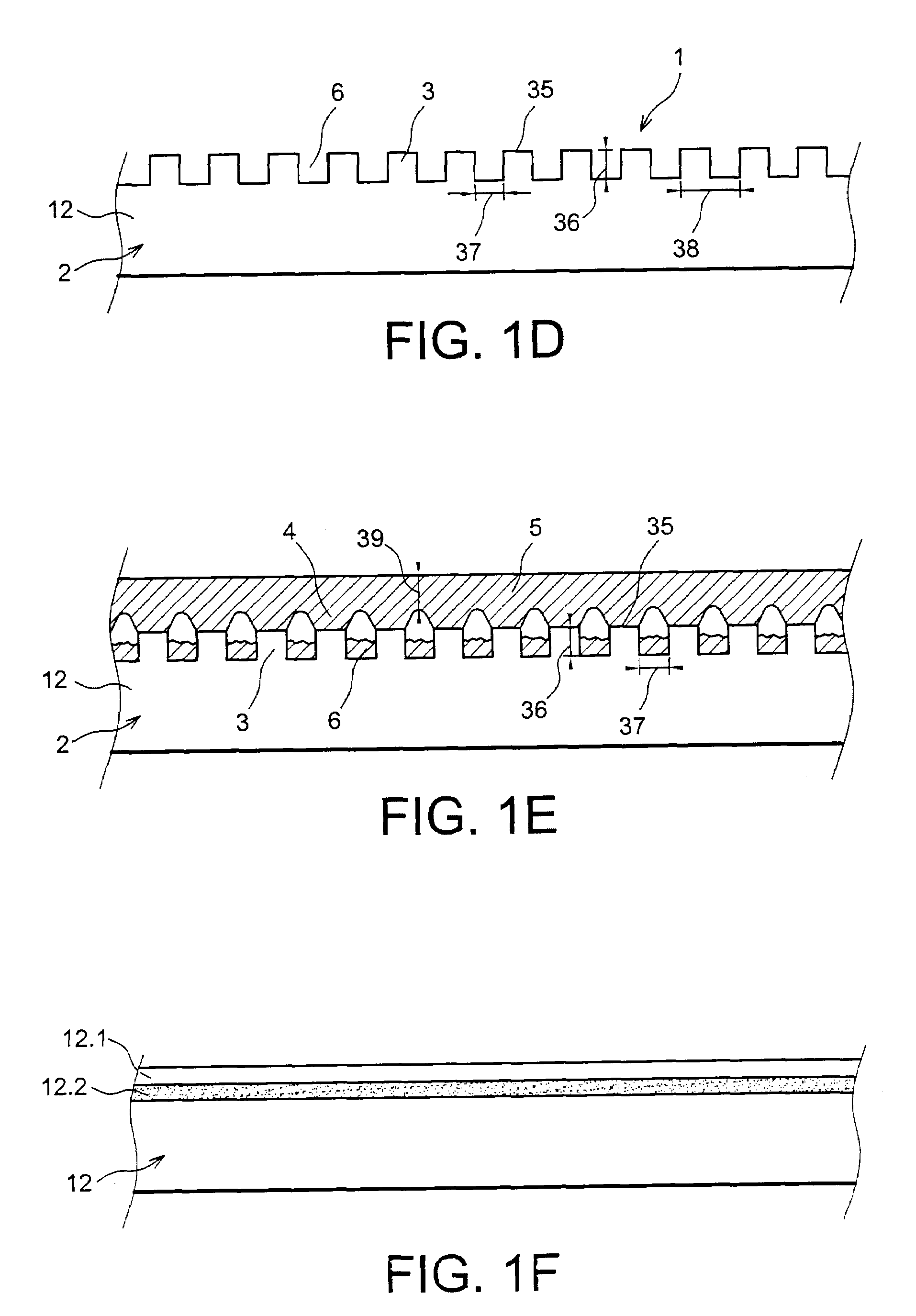
[0006]The present invention sets out to propose a method to produce an epitaxied structure by growing columns on a nanometric scale, without having to resort to a nanometric scale lithography step. This substrate is obtained economically and may have a large surface area. The position and geometry of the columns are obtained with great accuracy.

[0007]More precisely, the present invention is a method to produce an epitaxied structure, consisting of depositing a material by columnar epitaxial growth on a crystalline face of a substrate, of continuing deposit until the columns joint together and lead to a continuous layer. It consists of providing the face of the substrate with a periodic array of bumps on a nanometric scale, each bump having a support zone for a column, and being obtained directly or indirectly from an array of crystalline defects and / or strain fields created within a crystalline area located in the vicinity of a bonding interface between two elements comprising cryst...


PUM


Abstract

Method to produce a structure consisting of depositing a material by columnar epitaxy on a crystalline face of a substrate (2), of continuing so that the columns (4) give a continuous layer (5). The surface is provided with a period array of bumps (3) on a nanometric scale, each bump (3) having a support zone (35) and being obtained from an array of crystalline defects and/or strain fields created within a crystalline region (16) located in the vicinity of a bonding interface (15) between two crystalline elements (11, 12) whose crystalline lattices have a twist and/or tilt angle and/or have interfacial lattice mismatch, able to condition the period (38) of the array of bumps (3). The period (38) of the array, the height (36) of the bumps and the size of their support zone (35) being adjusted so that the continuous layer (40) has a critical thickness that is greater than that obtained using epitaxy without the bumps.

Description

TECHNICAL AREA[0001]The present invention relates to a method to produce an epitaxied structure. It is recalled that epitaxy is a technique to grow crystals which, on the surface of a host crystalline substrate, is used to form layers whose crystalline axes relate with the crystalline axes of the host substrate. The term heteroepitaxy is used if the deposited material is of different chemical species to the material of the host substrate. Substrates coated in this manner are of great advantage for the manufacture of semiconductor, optic or optoelectronic devices. Optimization of the crystalline growth of the layers can bring an improvement in the performance of these devices.STATE OF THE PRIOR ART[0002]Deposit by heteroepitaxy on a substrate generates misfit dislocations on and after a certain thickness of the deposited layer, called a critical thickness. This thickness depends on the difference in lattice parameters between the epitaxied material and the material of the host substr...

Claims


Application Information

Patent Timeline
Patent Type & Authority Applications(United States)
IPC IPC(8): H01L21/20H01L29/02
CPCC30B25/18C30B33/00H01L21/0237H01L21/02381H01L21/0243H01L21/02521H01L21/02639H01L21/0265H01L21/02664H01L21/187H01L21/30604
Inventor FOURNEL, FRANKMORICEAU, HUBERT
Owner COMMISSARIAT A LENERGIE ATOMIQUE ET AUX ENERGIES ALTERNATIVES
Why Eureka
Try Eureka