Antenna Device, Array Antenna, Multi-Sector Antenna, High-Frequency Wave Transceiver

a technology of array antenna and antenna gain, applied in the structure of individual energised antenna array, resonant antenna, radiating element, etc., can solve the problems of increasing transmission loss, antenna gain decline, and relative large space needed for each antenna device, so as to achieve superior antenna gain and reduce transmission loss

Inactive Publication Date: 2008-11-06
MURATA MFG CO LTD
View PDF7 Cites 33 Cited by
  • Summary
  • Abstract
  • Description
  • Claims
  • Application Information

AI Technical Summary

Benefits of technology

[0022]According to this invention, since a branch from a feeder electrode and unbalanced-balanced transform can be realized with two electrode branches provided at an interval of an odd multiple of ½ of a wavelength of a transmission / reception signal, an antenna device smaller than a conventional antenna can be formed. In particular, by setting the electrode branch position to ½ of the wavelength, a further smaller antenna device can be formed. In addition, since the antenna device is in such a shape, the transmission loss is reduced and an antenna device having a superior antenna gain can be formed.
[0023]In addition, according to this invention, by including a reflecting surface that forms a predetermined angle with a dielectric substrate on a side of the dielectric substrate different from the radiation electrode side, the transmission / reception directivity can be appropriately set and an antenna device having a desired characteristic can be formed in a small size.
[0024]Additionally, according to this invention, by connecting the antenna devices in series with a feeder electrode, an array antenna can be formed with a structure in which an integrated unit of a branch circuit to a radiation electrode of each antenna device and an unbalanced-balanced transform circuit is simply arranged along the feeder electrode. This allows the array antenna to be formed in a small size.
[0025]In addition, according to this invention, by using a plurality of array antennas, a multi-sector antenna can be formed in a small size. Furthermore, using these antenna devices, array antenna, and multi-sector antenna, a high-frequency wave transceiver can be formed in a small size.

Problems solved by technology

In addition, when an array antenna is formed using these antenna devices as shown in FIG. 12(C), a relatively large space is needed for each antenna device.
Thus, decreasing the space is problematic when an array antenna using a plurality of these antenna devices, a multi-sector antenna having this array antenna, and a high-frequency wave transceiver are miniaturized.
In addition, since the length of a transmission line connecting each unit becomes long, a transmission loss increases and an antenna gain decreases.

Method used


Image

  • Antenna Device, Array Antenna, Multi-Sector Antenna, High-Frequency Wave Transceiver
  • Antenna Device, Array Antenna, Multi-Sector Antenna, High-Frequency Wave Transceiver
  • Antenna Device, Array Antenna, Multi-Sector Antenna, High-Frequency Wave Transceiver

Examples


first embodiment

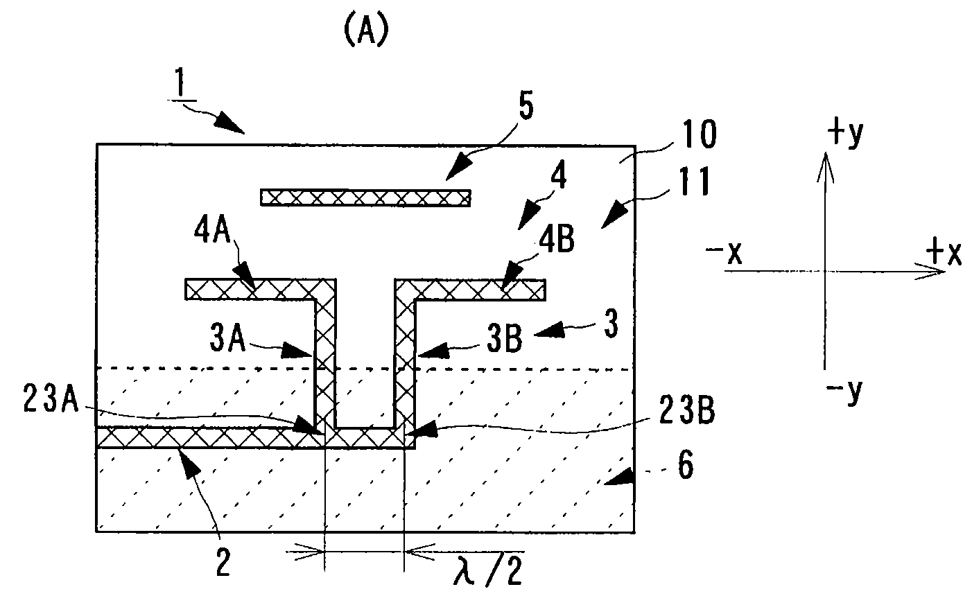
[0039]An antenna device according to the present invention will be described with reference to the drawings.

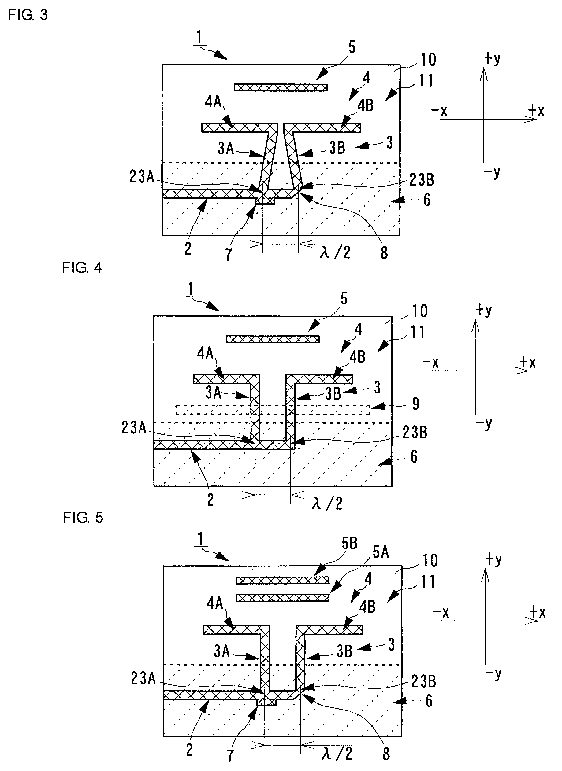
[0040]FIG. 1(A) is a plan view showing a structure of an antenna device 1 of this embodiment, whereas (B) is a side view thereof. In FIG. 1(A), the horizontal axis when viewed from the front is set as an x axis, whereas a direction toward the right and a direction toward the left are set as a +x direction and a −x direction, respectively. In addition, the vertical axis is set as a y axis, whereas an upward direction and a downward direction are set as a +y direction and a −y direction, respectively. In FIG. 1(B), the horizontal direction when viewed from the front is set as a z axis, whereas a direction toward the left and a direction toward the right are set as a +z direction and a −z direction, respectively. In addition, the vertical axis is set as a y axis, whereas an upward direction and a downward direction are set as a +y direction and a −y direction, respectively. Herei...

second embodiment

[0073]Next, an antenna device will be described with reference to the drawings.

[0074]FIG. 7(A) is an exterior perspective view of an antenna device 1′ of this embodiment, whereas (B) is a side view thereof. In addition, FIG. 7(C) is a side view showing a different structure of an antenna device of this embodiment.

[0075]In contrast to the antenna device 1 shown in FIG. 1, a conductor plate 61 is provided on a back surface 12 of a dielectric substrate 10 instead of the ground electrode 6 in the antenna device 1′ shown in FIG. 7. The structures on a top surface 11 of the dielectric substrate 10 are the same and the description regarding the top surface 11 is omitted.

[0076]The conductor plate 61 is formed in a shape substantially the size of the dielectric substrate 10 in a plan view of an x-y plane. A surface from one lateral face (a lateral face in the −y direction of FIG. 7) to a predetermined distance is formed like a plane (a planar portion 62). A surface from an end of this plana...

third embodiment

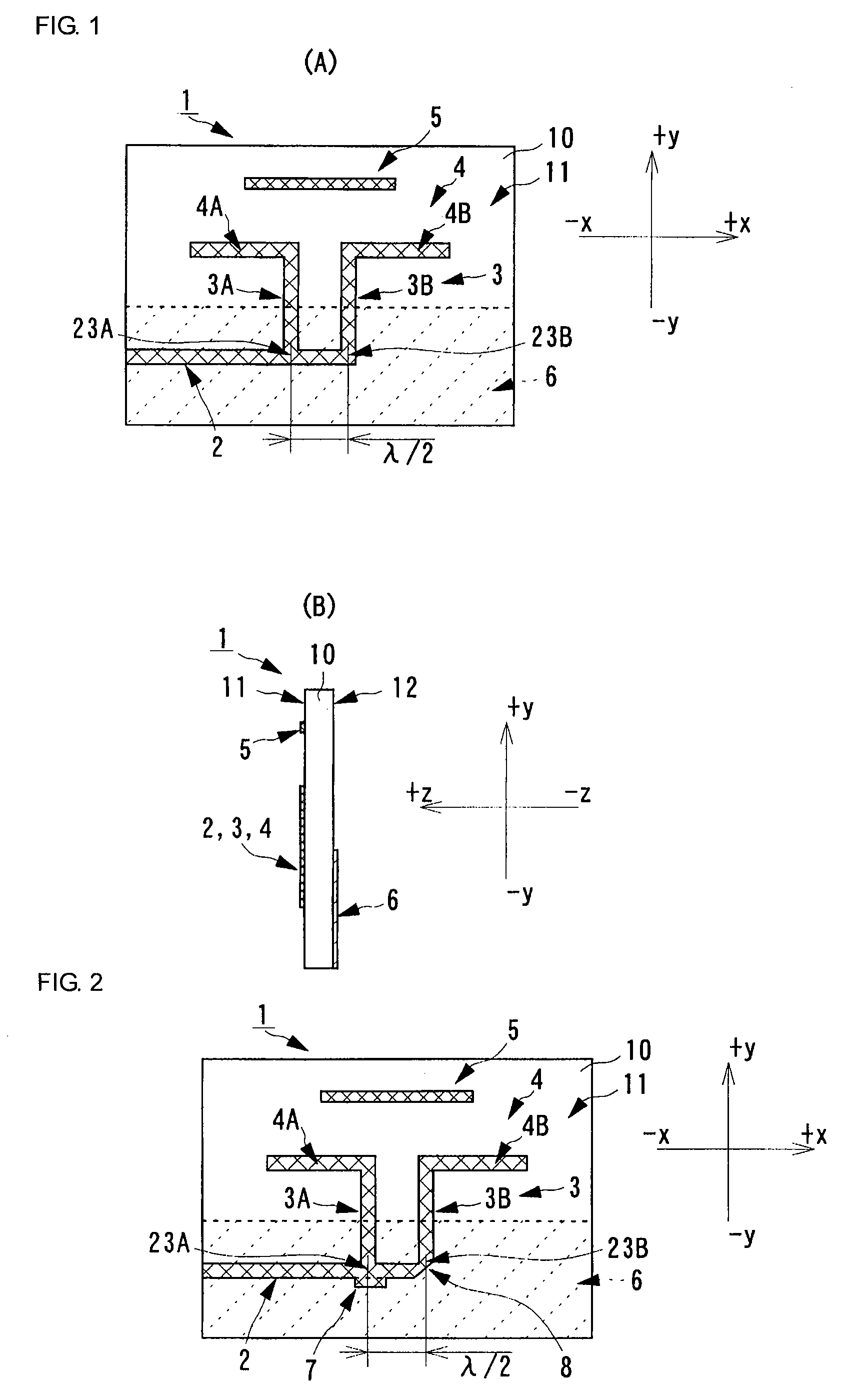
[0082]Next, an array antenna will be described with reference to the drawing.

[0083]FIG. 9 is a plan view showing a structure of an array antenna 200 of this embodiment.

[0084]As shown in FIG. 9, the array antenna 200 has a feeder electrode 2 extending linearly on the top surface of a dielectric substrate 10 in the x-axis direction. In addition, the array antenna 200 includes a balanced electrode, a radiation electrode, and a waveguide electrode for each of antenna devices 1A to 1C on the top surface of the dielectric substrate 10. Each of the antenna devices 1A to 1C is formed in the same shape as the above-described antenna device 1 shown in FIG. 3 except for the corner cut portion. In addition, in the array antenna 200, a junction position of the feeder electrode 2 and the balanced electrode of each of the antenna devices 1A to 1C is in a structure similar to the matching circuit 7 and the corner cut portion 8 shown in FIG. 3. Matching circuits 7A to 7C and a corner cut portion 8,...


PUM


Abstract

An antenna device having a feeder electrode that extends linearly on a top surface of a dielectric substrate. A balanced electrode having two balanced transmission electrodes vertical to the extending direction of the feeder electrode and extending in parallel. The two balanced transmission electrodes are connected to the feeder electrode and separated by an interval of ½ of a wavelength of a transmission/reception signal. A radiation electrode having a first electrode connected to the one of the two balanced transmission electrodes and a second electrode connected to the other of the two balanced transmission electrodes and is positioned parallel to the feeder electrode. A waveguide electrode is formed at a position separated from the radiation electrode by a predetermined interval and in parallel to the radiation electrode. A ground electrode is formed at an area of a back surface of the dielectric substrate corresponding to an area including a portion where the feeder electrode is positioned. By connecting the two balanced electrodes to the feeder electrode at an interval of ½ of a wavelength in this manner, this branch portion has a signal branching function and a balun function at the same time.

Description

CROSS REFERENCE TO RELATED APPLICATIONS[0001]The present application is a continuation of International Application No. PCT / JP2007 / 052958, filed Feb. 19, 2007, which claims priority to Japanese Patent Application No. JP2006-046749, filed Feb. 23, 2006, the entire contents of each of these applications being incorporated herein by reference in their entirety.FIELD OF THE INVENTION[0002]The present invention relates to antenna devices based on dipole antennas and, in particular, to a planar antenna device having dipole electrodes formed on a dielectric substrate. Furthermore, the present invention relates to an array antenna in which a plurality of these antenna devices are arranged, a multi-sector antenna having a plurality of array antennas, and a high-frequency wave transceiver.BACKGROUND OF THE INVENTION[0003]In the related art, Yagi-Uda antennas are one of antenna devices well known to the public. Such Yagi-Uda antennas include a planar type that employs a dielectric substrate in...

Claims


Application Information

Patent Timeline
Patent Type & Authority Applications(United States)
IPC IPC(8): H01Q9/16H01Q9/04
CPCH01Q9/285H01Q19/24H01Q19/30H01Q21/08
Inventor KITAMORI, NOBUMASANAGAI, TOMOHIRO
Owner MURATA MFG CO LTD
Why Eureka
Try Eureka