

Flip-chip semiconductor package and package substrate applicable thereto
- Summary
- Abstract
- Description
- Claims
- Application Information
AI Technical Summary
Benefits of technology
Problems solved by technology
Method used
Image

Examples
Embodiment Construction
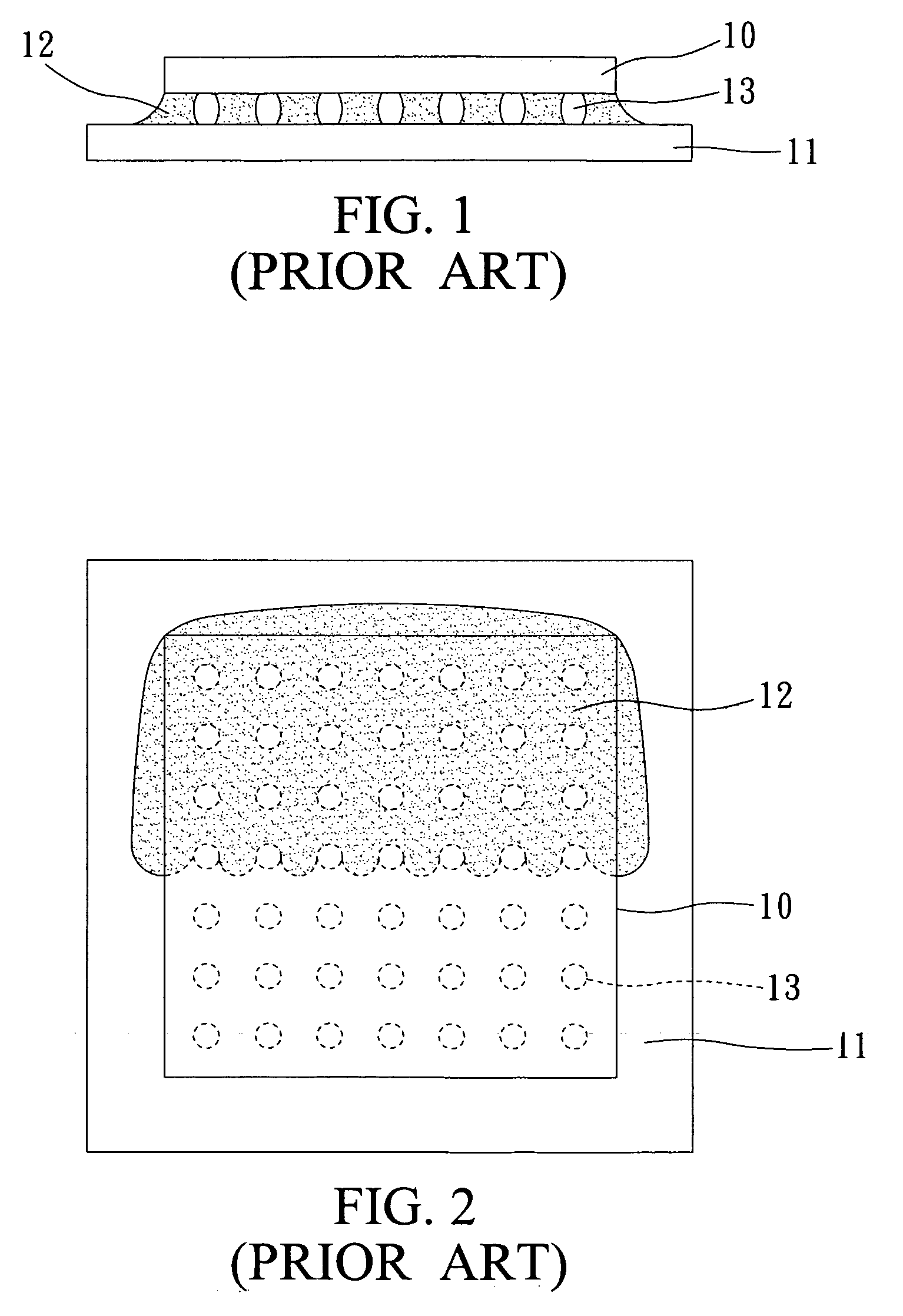
[0024]The following illustrative embodiments are provided to illustrate the disclosure of the present invention, these and other advantages and effects can be apparent to those skilled in the art after reading the disclosure of this specification. The present invention can also be performed or applied by other different embodiments. The details of the specification may be on the basis of different points and applications, and numerous modifications and variations can be made without departing from the spirit of the present invention.
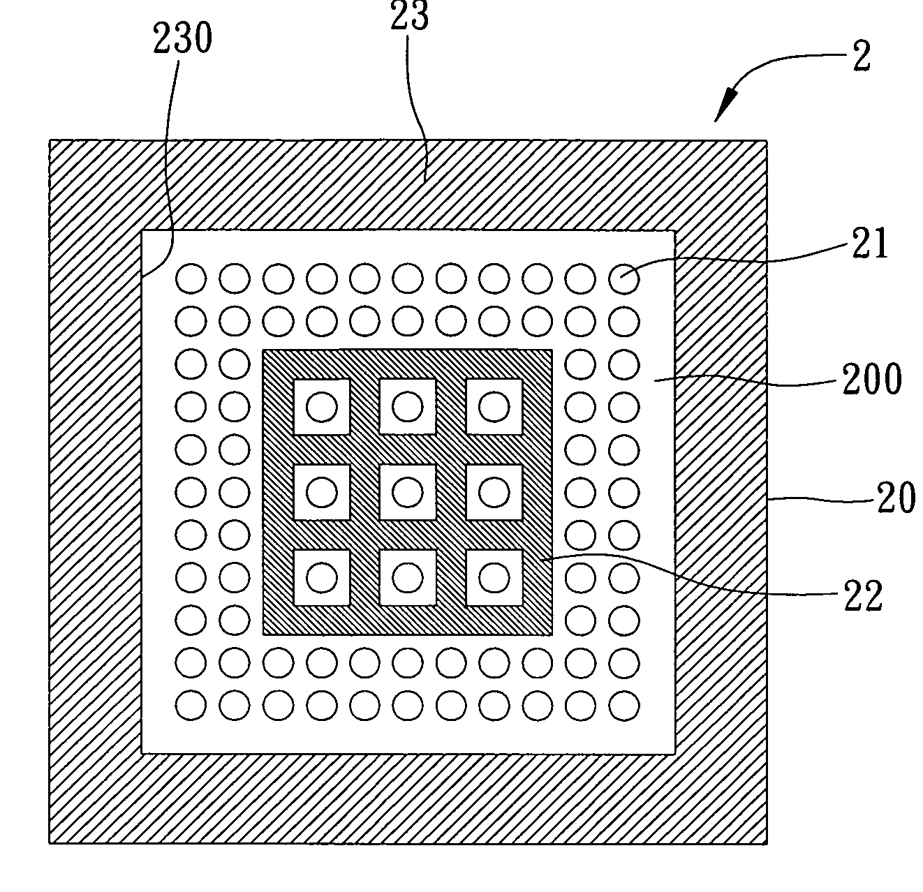
[0025]FIGS. 4A and 4B are diagrams of a package substrate applicable to a flip-chip semiconductor package structure according to the present invention, wherein FIG. 4B is sectional diagram of FIG. 4A.
[0026]The package substrate 2 comprises a body 20 having at least a chip-attach area 200 disposed thereon; a plurality of solder pads 21 disposed in the chip-attach area 200 and arranged at different intervals; and a fluid-disturbing portion 22 disposed in t...
PUM
 Abstract
Description
Claims
Application Information