Semiconductor integrated circuit

a technology of integrated circuits and semiconductors, applied in the direction of semiconductor devices, electrical equipment, transistors, etc., can solve the problems of large cell layout, difficult to predict the performance of a formed mos transistor, and large cell spacing,

Inactive Publication Date: 2008-11-20
KK TOSHIBA
View PDF6 Cites 54 Cited by
  • Summary
  • Abstract
  • Description
  • Claims
  • Application Information

AI Technical Summary

Benefits of technology

[0018]wherein an absolute value of threshold voltage of the dummy p-type MOS transistor is higher than an absolute value of threshold voltage of the p-type MOS transisto

Problems solved by technology

In other words, it is difficult to predict the performance of a formed MOS transistor.
However, a long distance from STI to the channel of the MOS transistor results in a large cell layout.
In the case where a semiconductor integrated circuit is designed by combining a plurality of function blocks called standard cells having uniform heights

Method used


Image

  • Semiconductor integrated circuit
  • Semiconductor integrated circuit
  • Semiconductor integrated circuit

Examples


first embodiment

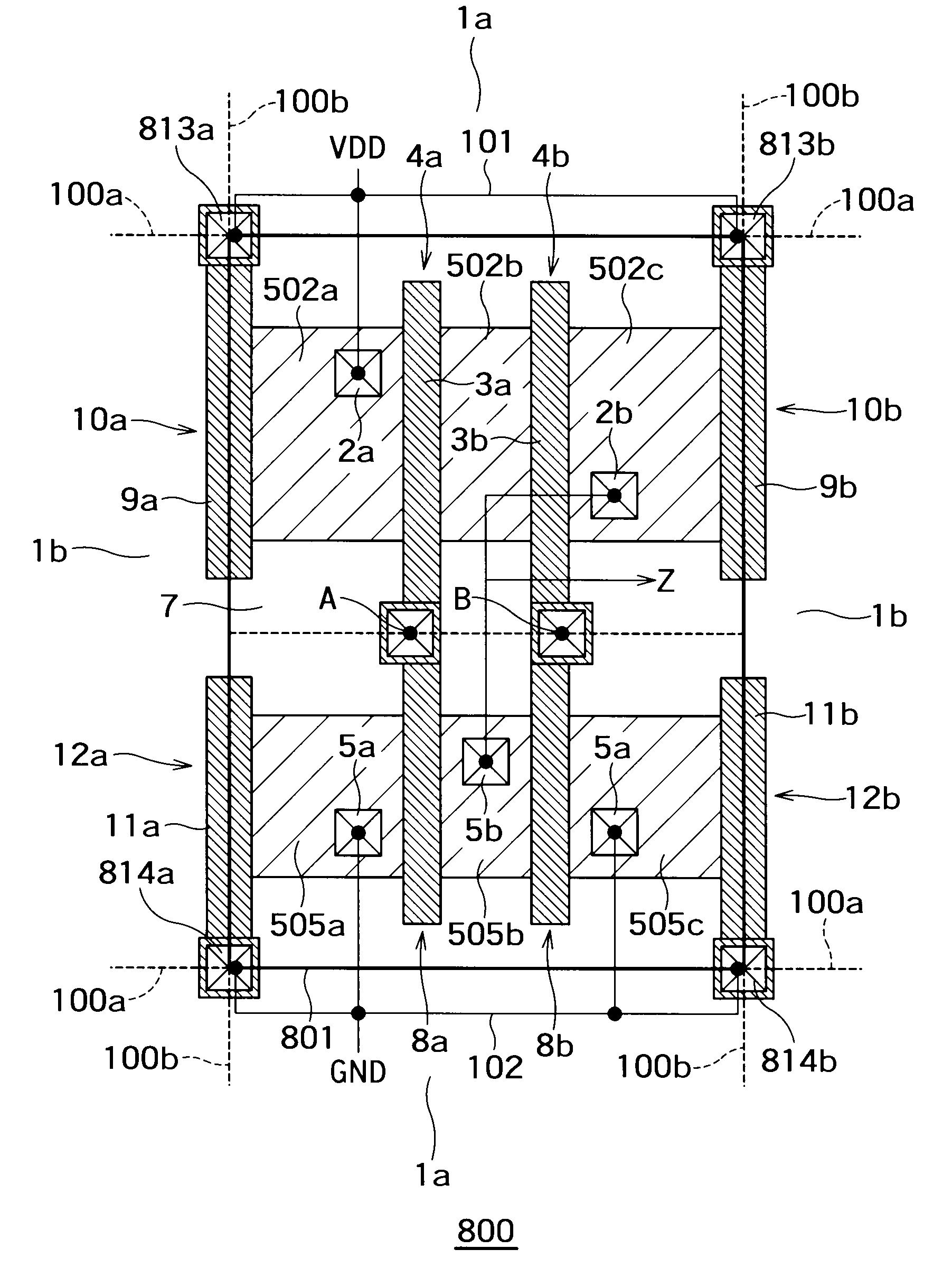
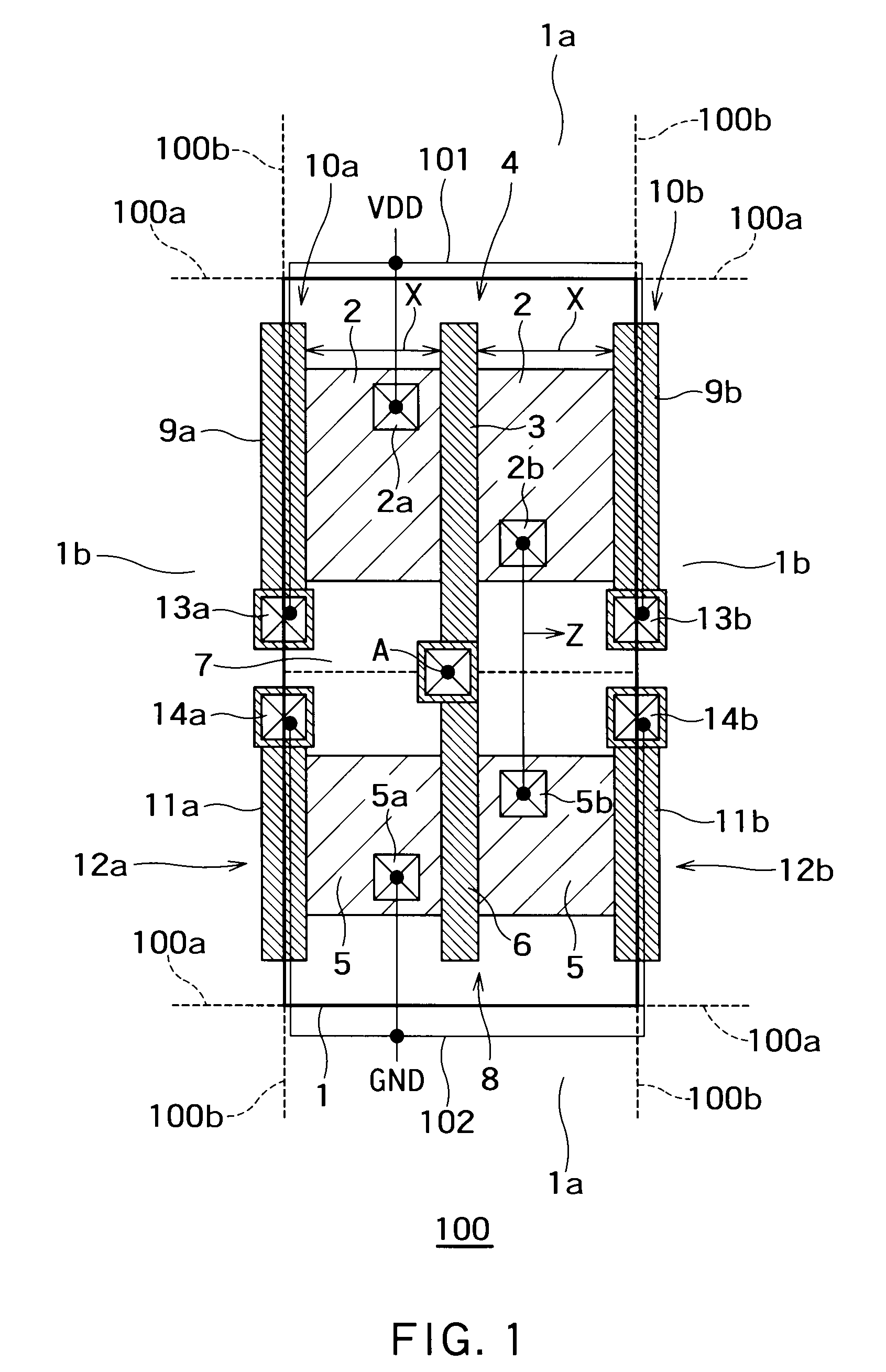
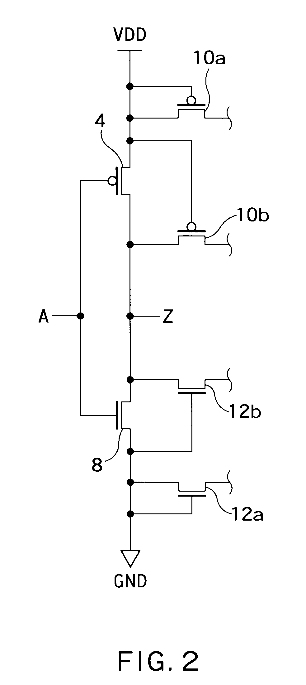
[0049]FIG. 1 shows the main configuration of a semiconductor integrated circuit 100 according to a first embodiment which is an aspect of the present invention. FIG. 2 is a circuit diagram showing the circuit configuration of a standard cell of the semiconductor integrated circuit 100 shown in FIG. 1.

[0050]As shown in FIG. 1, the semiconductor integrated circuit 100 has a substantially rectangular standard cell 1 which is divided by first borderlines 100a opposed to other standard cells 1a longitudinally adjacent to the standard cell 1, and second borderlines 100b opposed to other standard cells 1b laterally adjacent to the standard cell 1. In other words, in FIG. 1, the first borderlines 100a laterally extend and the second borderlines 100b longitudinally extend.

[0051]In FIG. 1, the detailed configurations of the standard cells 1a and 1b are omitted for the sake of simplicity (the same hereinafter). For example, the standard cell 1a and the standard cell 1b are identical in configu...

second embodiment

[0076]The first embodiment described an example of a standard cell including an inverter made up of MOS transistors.

[0077]The present embodiment will describe another example of a standard cell including an inverter made up of MOS transistors.

[0078]FIG. 3 shows the main configuration of a semiconductor integrated circuit 200 according to a second embodiment of the present invention.

[0079]In FIG. 3, the same reference numerals as those of FIG. 1 indicate the same configurations as those of the first embodiment. Further, in FIG. 3, the circuit configuration of the standard cell of the semiconductor integrated circuit 200 is identical to the circuit configuration of the circuit diagram shown in FIG. 2.

[0080]As shown in FIG. 3, the semiconductor integrated circuit 200 has a substantially rectangular standard cell 201 which is divided by first borderlines 100a opposed to other standard cells 1a longitudinally adjacent to the standard cell 201, and second borderlines 100b opposed to other...

third embodiment

[0092]The first and second embodiments described examples of a standard cell including an inverter made up of MOS transistors.

[0093]The present embodiment will describe still another example of a standard cell including an inverter made up of MOS transistors.

[0094]FIG. 4 shows the main configuration of a semiconductor integrated circuit 300 according to a third embodiment of the present invention.

[0095]In FIG. 4, the same reference numerals as those of FIG. 1 indicate the same configurations as those of the first embodiment. Further, in FIG. 4, the circuit configuration of the standard cell of the semiconductor integrated circuit 300 is identical to the circuit configuration of the circuit diagram shown in FIG. 2.

[0096]As shown in FIG. 4, the semiconductor integrated circuit 300 has a substantially rectangular standard cell 301 which is divided by first borderlines 100a opposed to other standard cells 1a longitudinally adjacent to the standard cell 301, and second borderlines 100b o...


PUM


Abstract

A semiconductor integrated circuit having a substantially rectangular standard cell divided by first borderlines opposed to other standard cells longitudinally adjacent to the standard cell and second borderlines opposed to other standard cells laterally adjacent to the standard cell, the standard cell has: a p-type MOS transistor having first diffused regions and a first gate electrode; an n-type MOS transistor having second diffused regions and a second gate electrode with STI disposed for device isolation between the n-type MOS transistor and the p-type MOS transistor substantially in parallel with the first borderlines; dummy p-type MOS transistors having third gate electrodes disposed on the second borderlines so as to be adjacent to the first diffused regions of the p-type MOS transistor, the third gate electrodes being connected to power supply wiring so as to turn off the dummy p-type MOS transistors; and dummy n-type MOS transistors having fourth gate electrodes disposed on the second borderlines so as to be adjacent to the second diffused regions of the n-type MOS transistor, the fourth gate electrodes being connected to ground wiring so as to turn off the dummy n-type MOS transistors.

Description

CROSS-REFERENCE TO RELATED APPLICATION[0001]This application is based upon and claims the benefit of priority from the prior Japanese Patent Application No. 2007-129537, filed on May 15, 2007, the entire contents of which are incorporated herein by reference.BACKGROUND OF THE INVENTION[0002]1. Field of the Invention[0003]The present invention relates to a semiconductor integrated circuit having a standard cell used for a cell-base design.[0004]2. Background Art[0005]In recent years, Shallow Trench Isolation (STI) for device isolation has been used in CMOS processes. It is known that because of finer design rules in the CMOS processes, the threshold values of CMOS transistors are affected by stresses caused by STI.[0006]For example, the shorter the distance from STI to the channel of a MOS transistor, the greater the stress of STI on the channel. Thus the current driving capability of an n-type MOS transistor decreases and the current driving capability of a p-type MOS transistor inc...

Claims


Application Information

Patent Timeline
IPC IPC(8): H01L29/76
CPCH01L27/0207H01L27/092H01L27/11807H01L2027/11831
Inventor HAMADA, MOTOTSUGU
Owner KK TOSHIBA
Why Eureka
Try Eureka