High frequency circuit, semiconductor device, and high frequency power amplification device

a high frequency circuit and high frequency power technology, applied in the direction of amplifiers, waveguide type devices, electrical equipment, etc., can solve the problems of increasing the output loss of the amplification device by the switching device, and achieve the effect of reducing loss and facilitating the switching of impedance and output path

Inactive Publication Date: 2008-11-20
PANASONIC SEMICON SOLUTIONS CO LTD
View PDF7 Cites 38 Cited by
  • Summary
  • Abstract
  • Description
  • Claims
  • Application Information

AI Technical Summary

Benefits of technology

[0010]A first aspect of the invention is a multifunctional, compact, high performance high frequency circuit that reduces loss caused by a switching d

Problems solved by technology

A problem with the related art thus described is that because a switching device must be connected before or a

Method used


Image

  • High frequency circuit, semiconductor device, and high frequency power amplification device
  • High frequency circuit, semiconductor device, and high frequency power amplification device
  • High frequency circuit, semiconductor device, and high frequency power amplification device

Examples


embodiment 1

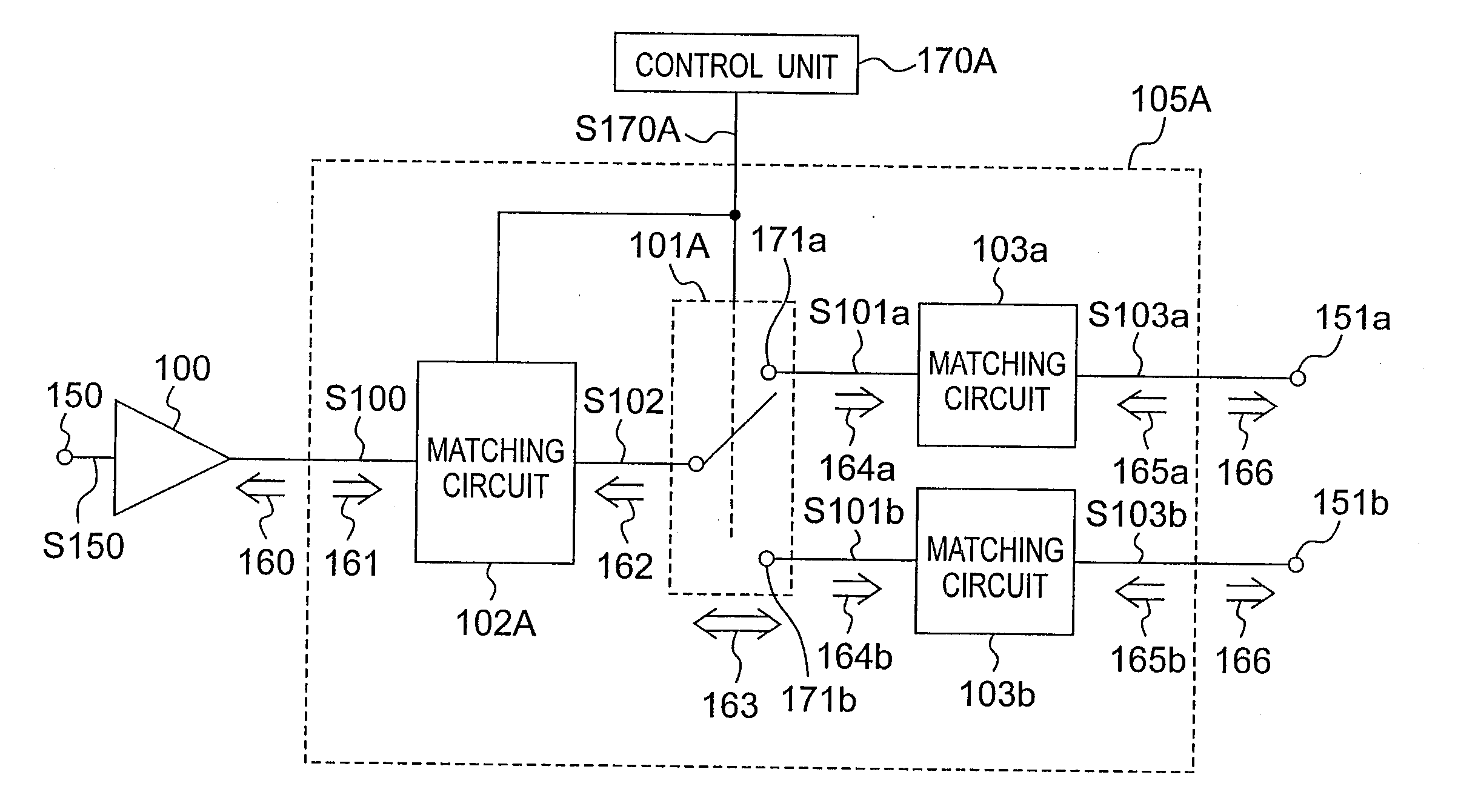
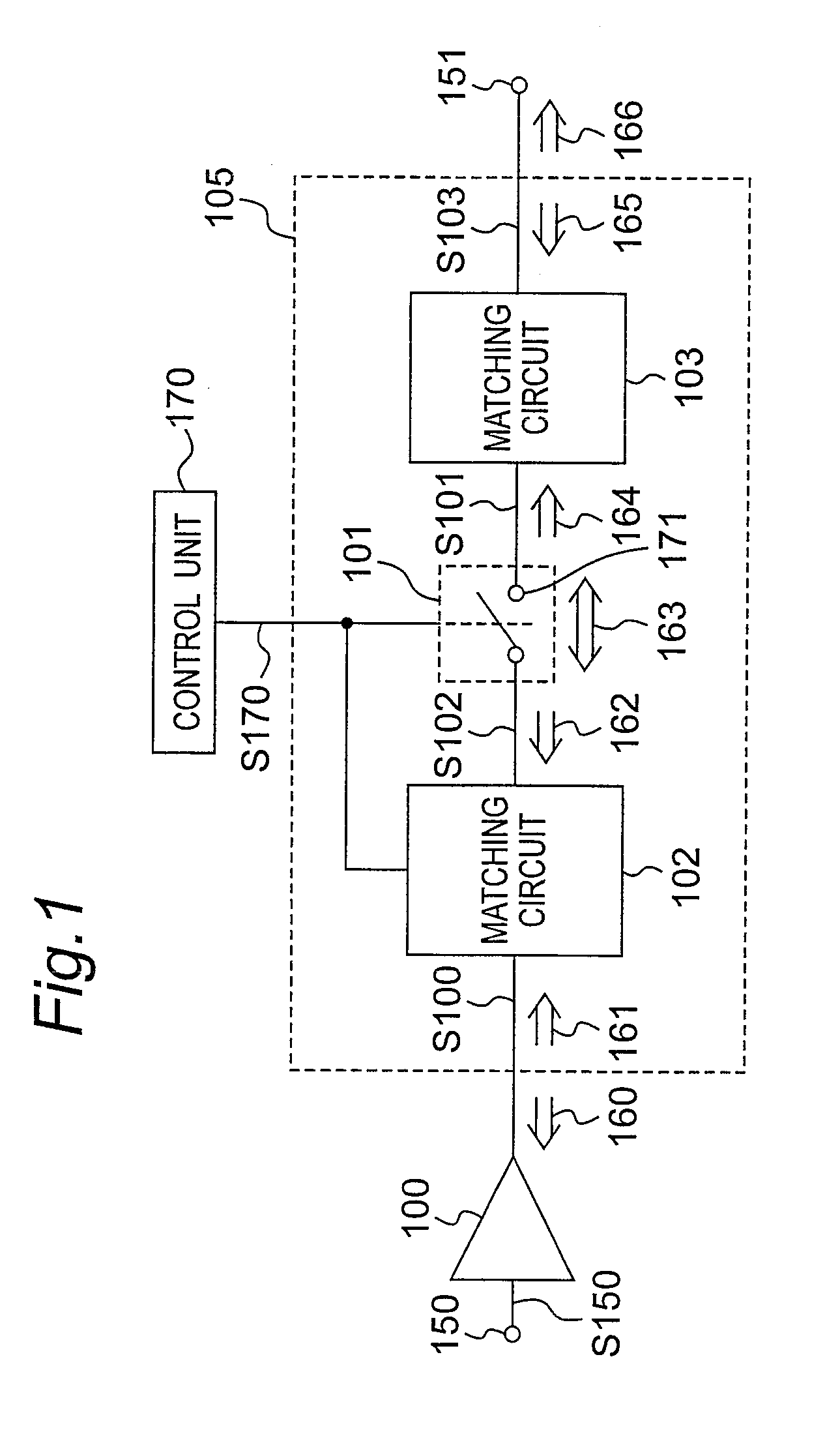
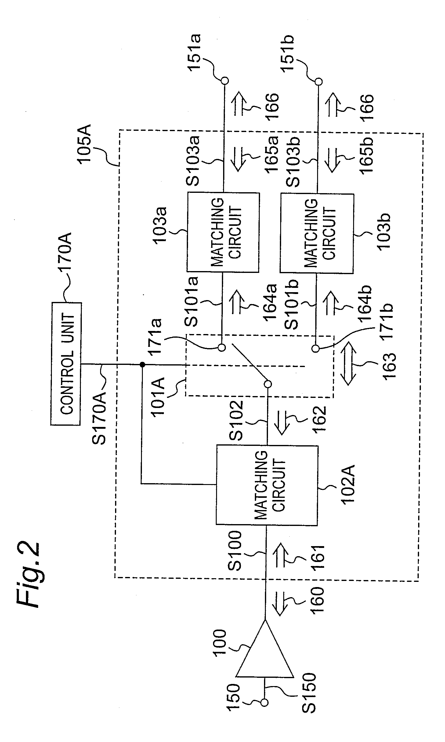
[0067]FIG. 2 is a block diagram of a high frequency circuit according to a first embodiment of the invention. The high frequency circuit according to this first embodiment of the invention includes an input pin 150, a final stage amplification unit 100, a matching circuit 102A, a switch unit 101A, matching circuits 103a and 103b, output pins 151a and 151b, and a control unit 170A.

[0068]The final stage amplification unit 100 amplifies the power of the input signal S150 input to the input pin 150, and outputs the amplified signal S100 at output impedance 160. The output impedance 160 is normally less than 50Ω. If the output of the final stage amplification unit 100 is high, such as when a 1-W input is boosted to several watts as in a cell phone, the output impedance 160 is generally approximately 3 to 8Ω.

[0069]The amplified signal S100 is input to the matching circuit 102A at an input impedance 161 substantially equal to a complex conjugate of the output impedance 160. More specifical...

embodiment 2

[0087]The second embodiment of the invention is described next with particular attention to the differences with the first embodiment. Other aspects of the arrangement, operation, and effect of this embodiment are the same as in the first embodiment, and further description thereof is omitted.

[0088]FIG. 5 is a block diagram of a high frequency circuit according to a second embodiment of the invention. The switch unit 101A of the first embodiment is replaced by a switch unit 101B in this second embodiment. The switch unit 101B is a single-pole, n-throw (where n is an integer of 3 or more) switch. The control unit 170B generates a control signal S170B denoting signal path selection information applied to the switch unit 101B. The matching circuit 102B controls the output impedance 162 based on control signal S170B. Also based on the control signal S170B, the switch unit 101B selects path 171a, 171b, to 171n and passes the impedance-converted signal S102 at on impedance 163 using the s...

embodiment 3

[0096]The third embodiment of the invention is described next with particular attention to the differences with the first embodiment. Other aspects of the arrangement, operation, and effect of this embodiment are the same as in the first embodiment, and further description thereof is omitted.

[0097]FIG. 6 is a circuit diagram showing an example of the matching circuit 102A in a third embodiment of the invention. The high frequency circuit in this third embodiment is identical to the high frequency circuit of the first embodiment shown in FIG. 2. FIG. 7A, FIG. 7B, and FIG. 7C are Smith charts showing the input / output impedance of selected parts in FIG. 2 and FIG. 6.

[0098]As described in the first embodiment, the matching circuit 102A controls the output impedance 162 based on the control signal S170A. To reduce insertion loss from the switch unit 101A, the matching circuit 102A sets the resistance component of the output impedance 162 sufficiently greater than the on impedance 163 and...


PUM


Abstract

A small, high performance, multifunctional high frequency circuit that is multiband and multimode compatible reduces loss from a switch formed on the output side of a final stage amplification unit. The final stage amplification unit power amplifies an input signal and outputs an amplified signal. A first matching circuit impedance converts the amplified signal input thereto at a first input impedance, and outputs a first impedance-converted signal at a first output impedance. A control unit that generates a control signal denoting signal path selection information. A switch unit selects one of at least two signal paths based on the control signal, passes the first impedance-converted signal at an on impedance through the selected path, and outputs the pass signal. A second matching circuit impedance converts a pass signal input thereto at a second input impedance, and outputs a second impedance-converted signal at a second output.

Description

BACKGROUND OF THE INVENTION[0001]1. Field of Invention[0002]The present invention relates to technology for a high frequency circuit that is used in mobile communication devices, for example, and to a high frequency power amplification device that uses the high frequency circuit, and relates more particularly to a high frequency circuit, to a semiconductor device, and to a high frequency power amplification device.[0003]2. Description of Related Art[0004]High frequency power amplifiers used in cell phones, for example, have an amplification device such as a transistor, an input matching circuit for efficiently inputting high frequency signals to the amplification device, and an output matching circuit for efficiently outputting high frequency signals from the amplification device. The matching circuits are composed of capacitors, inductors, microstrip lines, or other high frequency matching device, and are usually mounted on a circuit board as a semiconductor chip package. A semicon...

Claims


Application Information

Patent Timeline
IPC IPC(8): H03H7/38
CPCH03F1/56H03F3/189H03F2200/222H03F2200/255H03F2200/387H03F2200/423H03F2203/7233
Inventor TATEOKA, KAZUKIINAMORI, MASAHIKOMATSUDA, SHINGOOHASHI, KAZUHIKOKOIZUMI, HARUHIKO
Owner PANASONIC SEMICON SOLUTIONS CO LTD
Why Eureka
Try Eureka