Multi-Layer Flexible Printed Circuit Board and Method For Manufacturing the Same

a printed circuit board and flexible technology, applied in the direction of stacked and attached pcbs, synthetic resin layered products, chemistry apparatus and processes, etc., can solve the problems of poor influence on the camera module, difficulty in performing thin bonding between the fpcb and the electronic appliances, and increase the defect rate of the camera module, so as to reduce the defect rate of the target module bonded to the multi-layer fpcb and the effect of reducing the pressing time and improving heat con

Active Publication Date: 2008-11-27
LG INNOTEK CO LTD
View PDF9 Cites 7 Cited by
  • Summary
  • Abstract
  • Description
  • Claims
  • Application Information

AI Technical Summary

Benefits of technology

[0018]According to one embodiment of the present invention, a pressing / heating area of a multi-layer FPCB can be formed more thin as compared with that of the conventional multi-layer FPCB, so that heat conduction efficiency can be improved.
[0019]In addition, when the multi-layer FPCB is bonded to a target module, required pressing time can be reduced by 40% as compared with the pressing time of the conventional FPCB.
[0020]Further, the defect rate of the target module bonded to the multi-layer FPCB can be reduced.

Problems solved by technology

However, when the FPCB is connected to electronic appliances such as camera modules by using the ACF, the thickness of the FPCB and the ACF makes it difficult to perform the thin bonding between the FPCB and the electronic appliances.
In addition, since a heating temperature, a pressing pressure, and a bonding time interval increase proportionally to the thickness of the FPCB, a bad influence may be exerted on the camera module.
Accordingly, the defect rate of the camera modules may increase.

Method used


Image

  • Multi-Layer Flexible Printed Circuit Board and Method For Manufacturing the Same
  • Multi-Layer Flexible Printed Circuit Board and Method For Manufacturing the Same
  • Multi-Layer Flexible Printed Circuit Board and Method For Manufacturing the Same

Examples


Embodiment Construction

[0029]It will be understood that when an element is referred to as being ‘on’ or “under” a layer, it can be directly on / under the layer, and one or more intervening layers may also be present.

[0030]Hereinafter, a multi-layer FPCB according to an embodiment of the present invention will be described with reference to accompanying drawings.

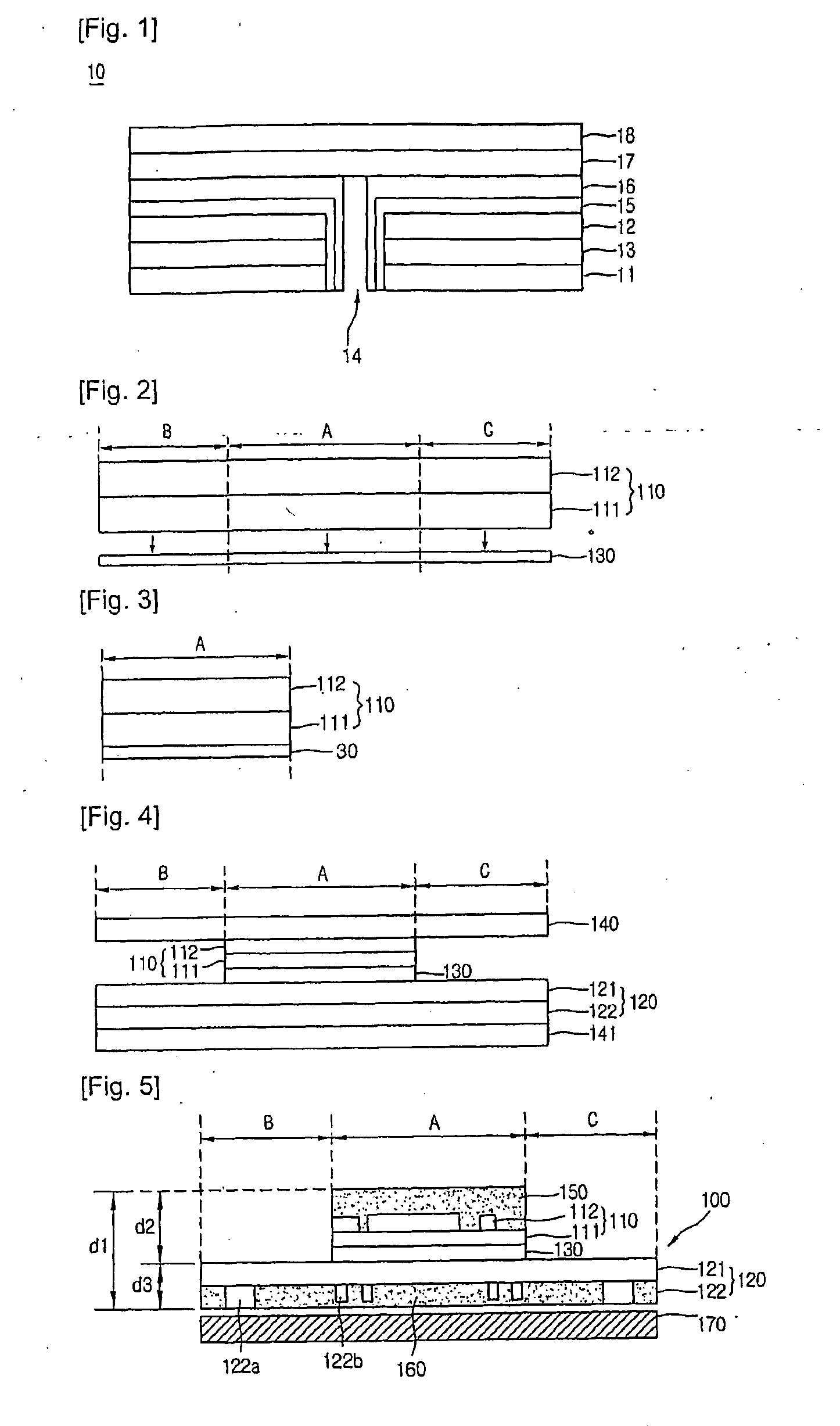
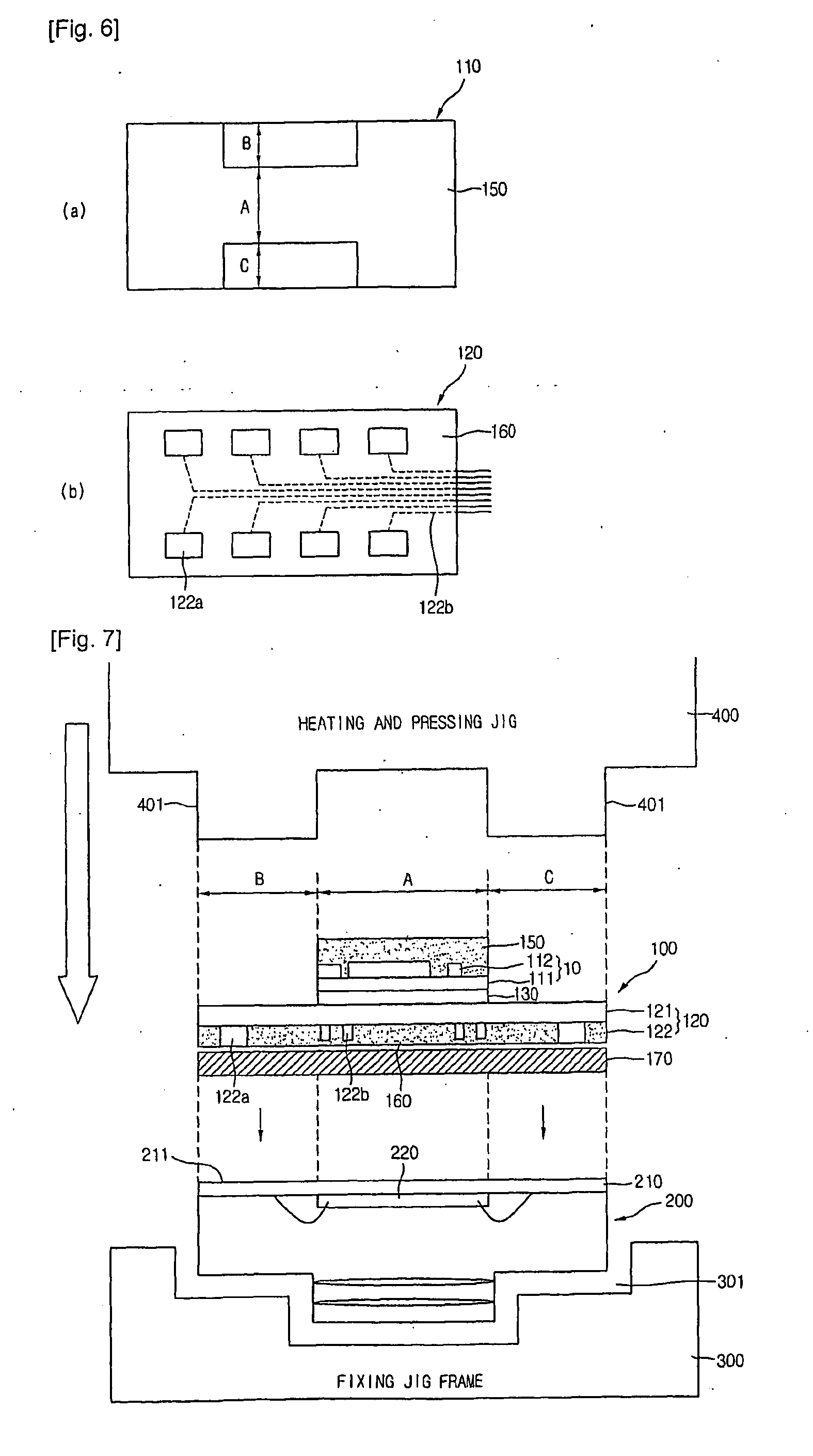
[0031]FIGS. 2 to 5 are views showing a manufacturing procedure of a multi-layer FPCB according to an embodiment of the present invention.

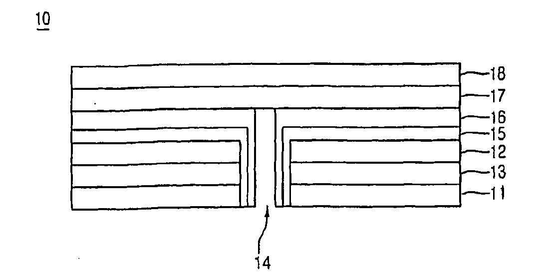
[0032]Referring to FIGS. 2 and 3, an upper base layer 110 includes a first insulating layer 111 and a first copper foil layer 112. The first insulating layer 111 includes insulating materials such as a flame retardant type 4 (FR-4) and a polyimide film, and the first copper foil layer 112 is bonded to a top surface of the first insulating layer 111 by an adhesive agent.

[0033]The upper base layer 110 is divided into a pattern forming area A and pressing / heating areas B and C. The pattern forming area A is used for f...


PUM

PropertyMeasurementUnit
thicknessaaaaaaaaaa
temperatureaaaaaaaaaa
flexibleaaaaaaaaaa

Abstract

Disclosed are a multi-layer flexible printed circuit board and a method for manufacturing the same. The multi-layer flexible printed circuit board includes an adhesion sheet from which a pressing and heating area is cut, an upper base layer, from which the pressing and heating area is cut, on the adhesion sheet, and a lower base layer under to the adhesion sheet.

Description

TECHNICAL FIELD[0001]The present invention relates to a multi-layer flexible printed circuit board and a method for manufacturing the same.BACKGROUND ART[0002]Recently, as electronic parts and component embedding technologies have been developed, and electronic appliances have become gradually light, compact, and slim, the demand of a multi-layer flexible printed circuit board (FPCB) is steadily growing.[0003]The multi-layer FPCB has strong heat-resistant, bending-resistant, and medicine-resistant characteristics, enables high-concentration interconnections, and is easily assembled with a device, so the multi-layer FPCB is widely used for cameras, computers, peripheral devices of the computers, mobile communication terminals, video and audio appliances, liquid crystal displays, satellite devices, medial devices, etc.[0004]In general, in order to manufacture the multi-layer FPCB, a dry film is laminated on a copper foil laminated film including a copper foil on a base film, and a pre...

Claims


Application Information

Patent Timeline
Patent Type & Authority Applications(United States)
IPC IPC(8): H05K1/00B29C65/72
CPCH05K1/0393H05K3/064H05K3/281H05K3/323H05K3/361H05K3/4611H05K3/4635H05K3/4691H05K3/4694H05K2201/0191H05K2201/0355H05K2201/043H05K2201/09127H05K2201/09972H01L2224/48091H01L2924/00014H05K3/46
Inventor LEE, HYUNG WOOK
Owner LG INNOTEK CO LTD
Why Eureka
Try Eureka