CMOS imaging device comprising a microlens array exhibiting a high filling rate

a microlens array and imaging device technology, applied in the field of cmos imagers, can solve the problems of poor imager yield (ratio between the received light energy and the light energy collected and transformed into electric voltage), poor quality of low-resolution image sensors, and low brightness of supplied images

Active Publication Date: 2008-11-27
STMICROELECTRONICS (ROUSSET) SAS +1
View PDF8 Cites 34 Cited by
  • Summary
  • Abstract
  • Description
  • Claims
  • Application Information

AI Technical Summary

Benefits of technology

[0022]In conclusion, the drawback of the above described conventional structure of microlenses is to have a fill factor far from the 100% ideal value, on the one hand because of the circular shape of the microlenses that limit filling in, and on the other hand because of the minimum separating distance εmin between the edges of microlenses.

Problems solved by technology

These CMOS imagers were initially used to manufacture low-resolution image sensors of poor quality (such as webcams).
Without microlens, the yield of the imager (ratio between the received light energy and the light energy collected and transformed into electric voltage) would be poor and the supplied images would have a low brightness and a low contrast.
Thus, despite the provision of the microlens array, 36% of the surface of each pixel is lost, i.e. 36% of the total surface of the imager.
This drawback is due to the circular shape of the base of the microlenses but also to the distance εmin between the edges of the adjacent microlenses.
In conclusion, the drawback of the above described conventional structure of microlenses is to have a fill factor far from the 100% ideal value, on the one hand because of the circular shape of the microlenses that limit filling in, and on the other hand because of the minimum separating distance εmin between the edges of microlenses.

Method used


Image

  • CMOS imaging device comprising a microlens array exhibiting a high filling rate
  • CMOS imaging device comprising a microlens array exhibiting a high filling rate
  • CMOS imaging device comprising a microlens array exhibiting a high filling rate

Examples


Embodiment Construction

Structure of a Microlens Array According to One Embodiment

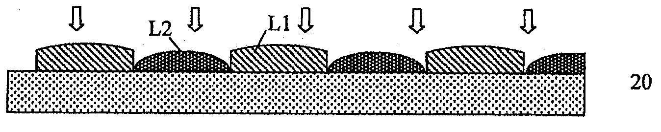
[0082]FIG. 6 is an abstract representation of a microlens array according to one embodiment, in top view. The shape of the microlenses in top view corresponds to the shape of the microlenses bases. The array comprises microlenses of a first type L1, or microlenses L1, made according to a first template G1, and microlenses of a second type L2, or microlenses L2, made according to a second template G2. The templates are shown in dotted lines whereas the microlenses bases are shown in continuous lines.

[0083]The microlens array has the following general features:[0084]the templates G1 and G2 are circles of radiuses R1 and R2 and are alternately arranged according to rows and columns of the array, indicated by horizontal and vertical dotted lines forming a network,[0085]the distance between the center of a microlens L1 and the center of an adjacent microlens L2 is equal to the pitch Pch of the photosite (pixel) array of the corres...


PUM


Abstract

A CMOS imager includes a photosite array and a microlens array. The microlens array comprises microlenses of a first type and microlenses of a second type, the microlenses of first type being manufactured according to a first circular template having a first radius, the microlenses of second type being manufactured according to a second circular template having a second radius inferior to the first radius, and the first and second templates having overlap areas. One advantage is that the CMOS imager has a high fill rate.

Description

CROSS-REFERENCE TO RELATED APPLICATION[0001]This application is a continuation-in-part of International Patent Application No. PCT / FR2006 / 002581, filed Nov. 24, 2006, now pending, which application is incorporated herein by reference in its entirety.[0002]This application claims the benefit under 35 U.S.C. § 119(a) of French Patent No. 05 12137, filed on Nov. 30, 2005, which application is incorporated herein by reference in its entirety.BACKGROUND[0003]1. Technical Field[0004]The present invention relates to CMOS imagers and more particularly to a structure of microlens array of CMOS imager and to a method for manufacturing this microlens array.[0005]2. Description of the Related Art[0006]Imagers manufactured according to the CMOS technology (“Complementary Metal Oxide Semiconductor”) are currently used in an increasing number of applications due to their low cost price compared to CDD imagers (Charge Coupled Device). These CMOS imagers were initially used to manufacture low-resolu...

Claims


Application Information

Patent Timeline
Patent Type & Authority Applications(United States)
IPC IPC(8): H01L31/00H01L21/00
CPCG02B3/0018G02B3/0056H01L27/14627H01L27/14643H01L27/14685
Inventor DUNNE, BRENDANFOSSATI, CAROLINEGAGLIANO, OLIVIER
Owner STMICROELECTRONICS (ROUSSET) SAS
Why Eureka
Try Eureka