Semiconductor device

a technology of semiconductor devices and semiconductor substrates, applied in semiconductor devices, semiconductor/solid-state device details, electrical apparatus, etc., can solve the problems of cracking at the junction portions between the ceramic substrate and the back side metal layer, and reducing heat radiating performance, so as to prevent cracks and peeling, the effect of superior heat radiating performan

Inactive Publication Date: 2008-11-27
TOYOTA IND CORP +1
View PDF0 Cites 25 Cited by
  • Summary
  • Abstract
  • Description
  • Claims
  • Application Information

AI Technical Summary

Benefits of technology

[0007]Accordingly, it is an objective of the present invention to provide a semiconductor device that...

Problems solved by technology

However, depending on the use conditions, cracks may occur at junction portions between the ceramic substrate and the back side metal layer due to thermal stress generated by the difference in coefficient of linear expansion between the metal layer a...

Method used


Image

  • Semiconductor device
  • Semiconductor device
  • Semiconductor device

Examples


Embodiment Construction

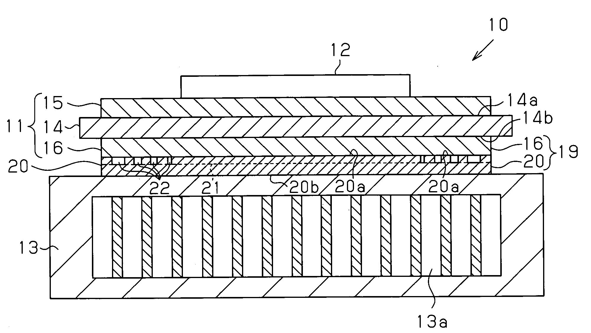
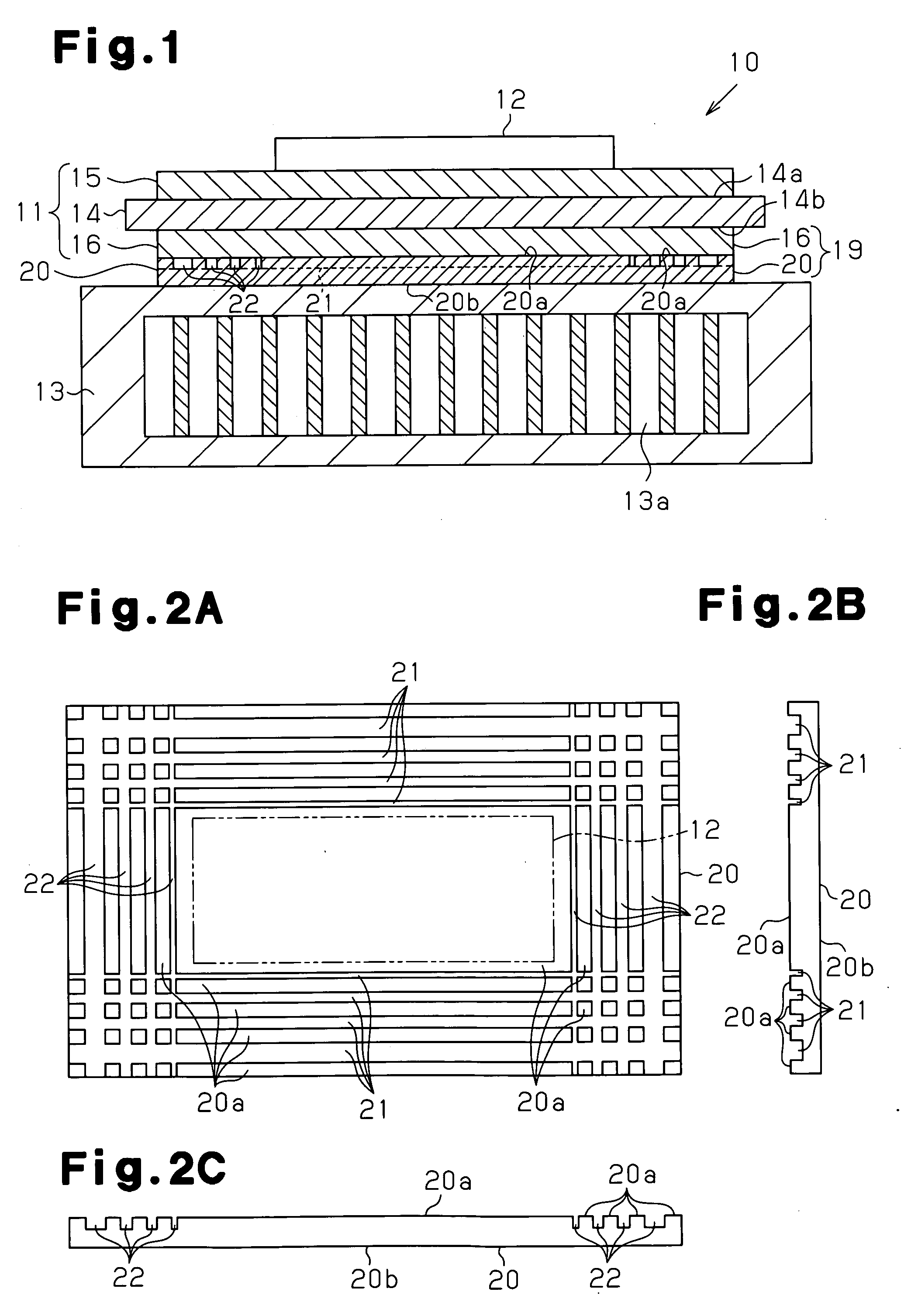
[0020]One embodiment of the present invention will now be described with reference to FIGS. 1 to 3.

[0021]As shown in FIG. 1, a semiconductor device 10 includes a circuit board 11, a semiconductor element 12 joined to the circuit board 11, a heat sink 13 functioning as a radiator, and a stress relaxation member 20 located between the circuit board 11 and the heat sink 13. The circuit board 11 is provided with a ceramic substrate (insulated substrate) 14 that has a first surface 14a (front side) and a second surface 14b (back side), which is opposite to the first surface 14a. The circuit board 11 also includes a metal circuit 15, which is directly joined to the first surface 14a, and a metal plate 16, which is directly joined to the second surface 14b. The semiconductor element 12 is joined to the metal circuit 15, so that the semiconductor element 12 and the ceramic substrate 14 are coupled to each other by the metal circuit 15.

[0022]The semiconductor element 12 may be, for example, ...


PUM


Abstract

A semiconductor device is disclosed that includes a ceramic substrate having first and second surfaces, a semiconductor element, a radiator, and an interposed portion located between the second surface and the radiator. The interposed portion has coupling regions that couple the second surface to the radiator, and non-coupling regions that do not couple the second surface to the radiator. Each non-coupling region is formed as an elongated groove. In the group of the non-coupling regions, the width of the outermost non-coupling region in the interposed portion is greater than the width of the innermost non-coupling region in the interposed portion. Regarding an adjacent pair of the non-coupling regions in the width direction, the width of the outer non-coupling region is greater than or equal to the width of the inner non-coupling region.

Description

BACKGROUND OF THE INVENTION[0001]The present invention relates to a semiconductor device including a ceramic substrate that has a first surface, to which a semiconductor element is coupled, and a second surface, to which a radiator is coupled.[0002]Conventionally, modularized semiconductor devices are known. In such a semiconductor device, metal layers are respectively provided on both of the front and back sides of a ceramic substrate, which is, for example, made of aluminum nitride. A semiconductor element is coupled (joined) to the front side metal layer, and a heat sink (radiator) is coupled (joined) to the back side metal layer. The heat sink radiates heat generated by the semiconductor element. Semiconductor devices are required to maintain heat radiating performance of the heat sink for an extended period of time. However, depending on the use conditions, cracks may occur at junction portions between the ceramic substrate and the back side metal layer due to thermal stress ge...

Claims


Application Information

Patent Timeline
IPC IPC(8): H01L23/34
CPCH01L23/13H01L23/3735H01L23/473H01L2924/13055H01L2924/13091H01L24/32H01L2924/1305H01L2924/1306H01L2924/00H01L2924/351H01L2924/15787H01L2224/2612H01L23/36
Inventor NISHI, SHINSUKEWATANABE, SHINTAROMORI, SHOGONAKAGAWA, SHINTAROSUZUYAMA, TAKESHIICHIYANAGI, SHIGEHARU
Owner TOYOTA IND CORP
Why Eureka
Try Eureka