Semiconductor device and method of manufacturing the same and data processing system

a semiconductor device and data processing system technology, applied in the field of semiconductor devices, can solve the problems of inability to meet the requirements of the market, the semiconductor device does not operate correctly, and the transistor characteristics fluctuate accordingly, so as to ensure high reliability, connect reliably, and stable transistor characteristics

Inactive Publication Date: 2008-12-04
ELPIDA MEMORY INC
View PDF6 Cites 37 Cited by
  • Summary
  • Abstract
  • Description
  • Claims
  • Application Information

AI Technical Summary

Benefits of technology

[0015]Further, even if the planar size of the silicon pillar is very small, the silicon pillar and the upper wiring can be connected reliably.
[0016]Furthermore, a insulation between the gate electrode and the conductive film formed on the upper part of the silicon pillar can be ensure reliably.
[0017]As explained above, according to the present invention, stable transistor characteristics and highly reliability can be ensured.

Problems solved by technology

However, miniaturization of transistors has come to the limit, and when the transistors are attempted to be more miniaturized, there is a risk that the semiconductor device does not operate correctly due to the short-channel effect and the like.
As a result, a problem that transistor characteristics fluctuate occurs accordingly.
However, it is difficult to expose the upper portion of the silicon pillar because a planar area of the silicon pillar is designed very small.
This results in deterioration of reliability of products.

Method used


Image

  • Semiconductor device and method of manufacturing the same and data processing system
  • Semiconductor device and method of manufacturing the same and data processing system
  • Semiconductor device and method of manufacturing the same and data processing system

Examples


Embodiment Construction

[0059]Preferred embodiments of the present invention will now be described in detail hereinafter with reference to the accompanying drawings.

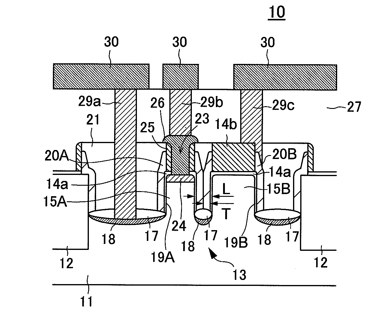
[0060]FIGS. 1A and 1B are a schematic cross-sectional view and a schematic top plan view, respectively showing a structure of a semiconductor device 10 according to a preferred embodiment of the present invention.

[0061]As shown in FIGS. 1A and 1B, the semiconductor device 10 according to the present embodiment is a vertical transistor using a silicon pillar, and includes an STI (Shallow Trench Isolation) 12 formed on a silicon substrate 11, first and second silicon pillars 15A and 15B formed in an active region encircled by the STI 12, a first gate electrode 20A covering a side surface of the first silicon pillar 15A via a first gate insulation film 19A, and a second gate electrode 20B covering a side surface of the second silicon pillar 15B via a second gate insulation film 19B. The semiconductor device 10 also includes a first diffusion layer...


PUM


Abstract

A semiconductor device is provided with a silicon pillar formed substantially perpendicularly to a main surface of a substrate, a gate electrode covering side surface of the silicon pillar via a gate insulation film, a conductive layer provided on an upper part of the silicon pillar, a cylindrical sidewall insulation film intervening between the conductive layer and the gate electrode so as to insulate therebetween. An inner wall of the side wall insulation film is in contact with the conductive layer, and an outer wall of the side wall insulation film is in contact with the gate electrode.

Description

TECHNICAL FIELD[0001]The present invention relates to a semiconductor device and a method of manufacturing the same, and more particularly relates to a semiconductor device having a vertical transistor using a silicon pillar, and a method of manufacturing the semiconductor device. The present invention also relates to a data processing system including semiconductor device having a vertical transistor using a silicon pillar.BACKGROUND OF THE INVENTION[0002]The integration of the semiconductor device has hitherto been achieved mainly by miniaturizing transistors. However, miniaturization of transistors has come to the limit, and when the transistors are attempted to be more miniaturized, there is a risk that the semiconductor device does not operate correctly due to the short-channel effect and the like.[0003]As a method of basically solving this problem, there has been proposed a method of three-dimensionally processing a semiconductor substrate, thereby three-dimensionally forming ...

Claims


Application Information

Patent Timeline
Patent Type & Authority Applications(United States)
IPC IPC(8): H01L29/78H01L21/4763
CPCH01L29/66666H01L29/7827
Inventor TAKAISHI, YOSHIHIRO
Owner ELPIDA MEMORY INC
Why Eureka
Try Eureka