Semiconductor test apparatus

a test apparatus and semiconductor technology, applied in the direction of electrical testing, measurement devices, instruments, etc., can solve the problems of complicated configuration of the probe assembly including the probe card b>4/b>, and achieve the effect of simplifying the configuration of the test apparatus, shortening the circuit length, and reducing costs

Inactive Publication Date: 2008-12-04
NIHON MICRONICS
View PDF4 Cites 31 Cited by
  • Summary
  • Abstract
  • Description
  • Claims
  • Application Information

AI Technical Summary

Benefits of technology

[0021]According to the present invention, as described above, by directly connecting the electrical connection portion of the tester to the probe card, the constitution of the test apparatus can be simplified, and cos

Problems solved by technology

Thus, the constitution of the probe assembl

Method used


Image

  • Semiconductor test apparatus
  • Semiconductor test apparatus
  • Semiconductor test apparatus

Examples


Embodiment Construction

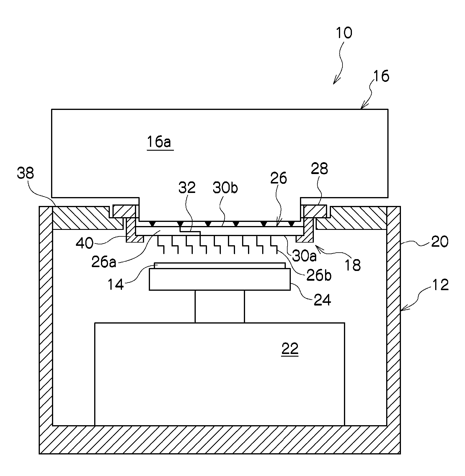
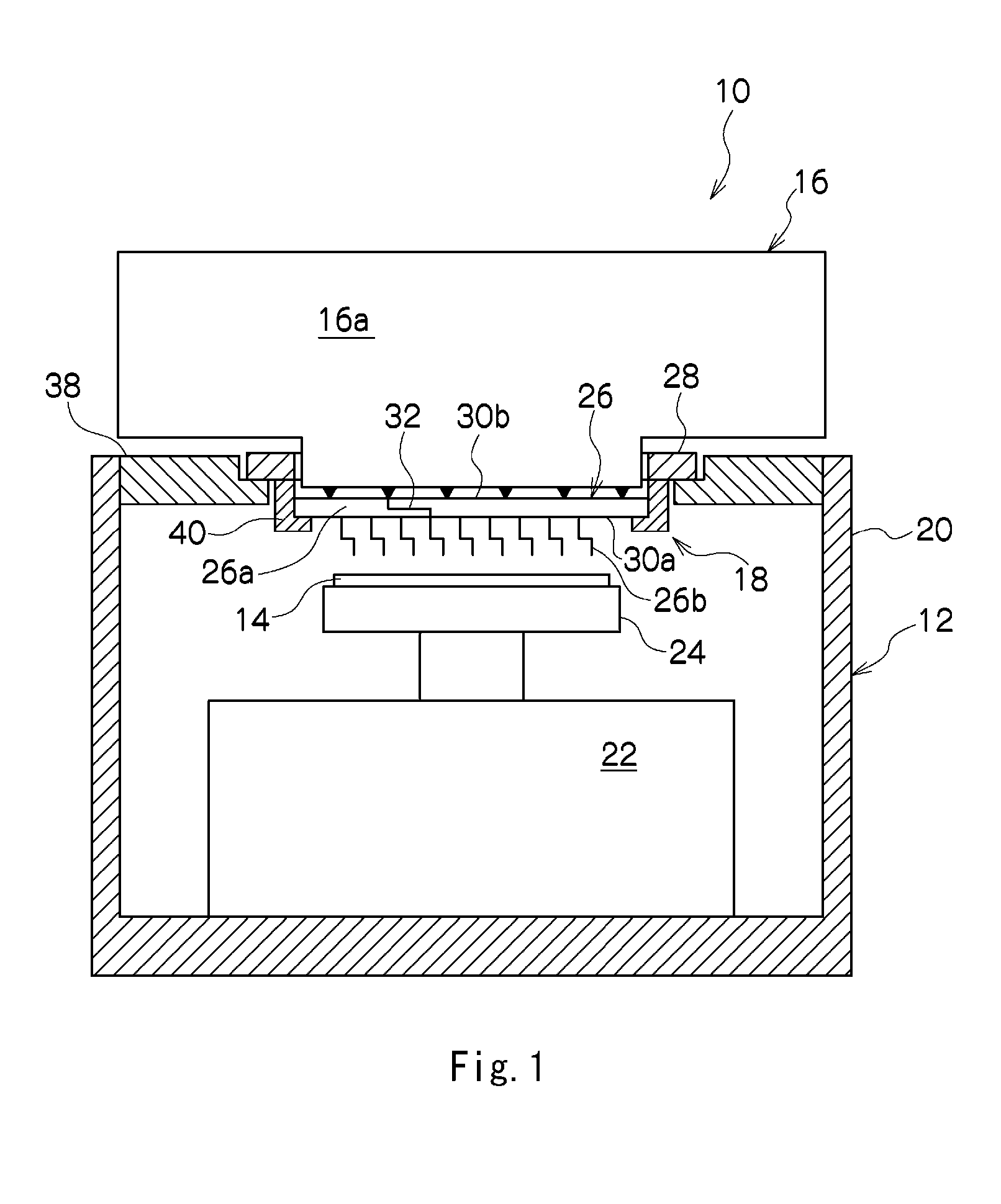
[0030]A test apparatus 10 according to the present invention comprises a wafer prober 12 as a prober mechanism, a tester 16 for conducting an electrical test of a semiconductor wafer 14 supported by the wafer prober, and a probe assembly 18 for electrically connecting the tester to the semiconductor wafer 14, as shown in FIG. 1.

[0031]The wafer prober 12 comprises an entirely rectangular casing 20 and a chuck top 24 held on a test stage 22 arranged in the casing. The semiconductor wafer 14 has numerous integrated circuits incorporated therein and is removably held on the chuck top 24 with their electrodes directing upward. The test stage 22 is combination of X, Y, Z, and theta stages as is conventionally well known, and the chuck top 24 enables positional adjustment in an X direction and a Y direction perpendicular to this on the horizontal plane, in a vertical direction (Z direction) perpendicular to the horizontal plane (XY plane), and in a rotating direction (theta) around the Z a...


PUM


Abstract

The present invention provides a semiconductor test apparatus that can reduce influence of noise in high-frequency measurement and that can be manufactured inexpensively by simplification of the constitution. A semiconductor test apparatus according to the present invention is one for use in an electrical test of a semiconductor wafer in which numerous integrated circuits each having electrode pads are incorporated. It comprises a probe card and a tester having a connection portion to the probe card. The probe card has numerous probes that can be connected to the electrode pads of the semiconductor wafer and a probe board having on one surface probe lands to which the probes are attached, having on the other surface tester lands corresponding to the probes, and having wiring paths each connecting the probe land and the tester land corresponding to each other. The tester is directly connected to the probe card as the connection portion contacts the tester lands.

Description

BACKGROUND OF THE INVENTION[0001]The present invention relates to a semiconductor test apparatus for use in an electrical test of a semiconductor wafer in which numerous integrated circuits are incorporated.[0002]In an electrical test of numerous integrated circuits incorporated in a semiconductor wafer is generally used a test apparatus comprising a tester and a probe card provided with numerous probes that connect the tester to respective electrode pads of the integrated circuits as devices under test (for example, refer to Patent Document 1).[0003]A test apparatus 1 of this kind comprises a probe card 4 provided with probes 4a that can be connected to electrode pads of a semiconductor wafer 3 as a device under test held on a chuck 2a of a prober apparatus 2, as shown in FIG. 8.[0004]The probe card 4 is opposed to the lower surface of a wiring board 5 and is attached to the wiring board. Also, the edge portion of the probe card 4 is held by the wiring board 5 via an annular holdin...

Claims


Application Information

Patent Timeline
IPC IPC(8): G01R1/073
CPCG01R1/06772G01R1/07364G01R31/2886
Inventor MIURA, KIYOTOSHIINOUE, TATSUOWASHIO, KENICHI
Owner NIHON MICRONICS
Why Eureka
Try Eureka