

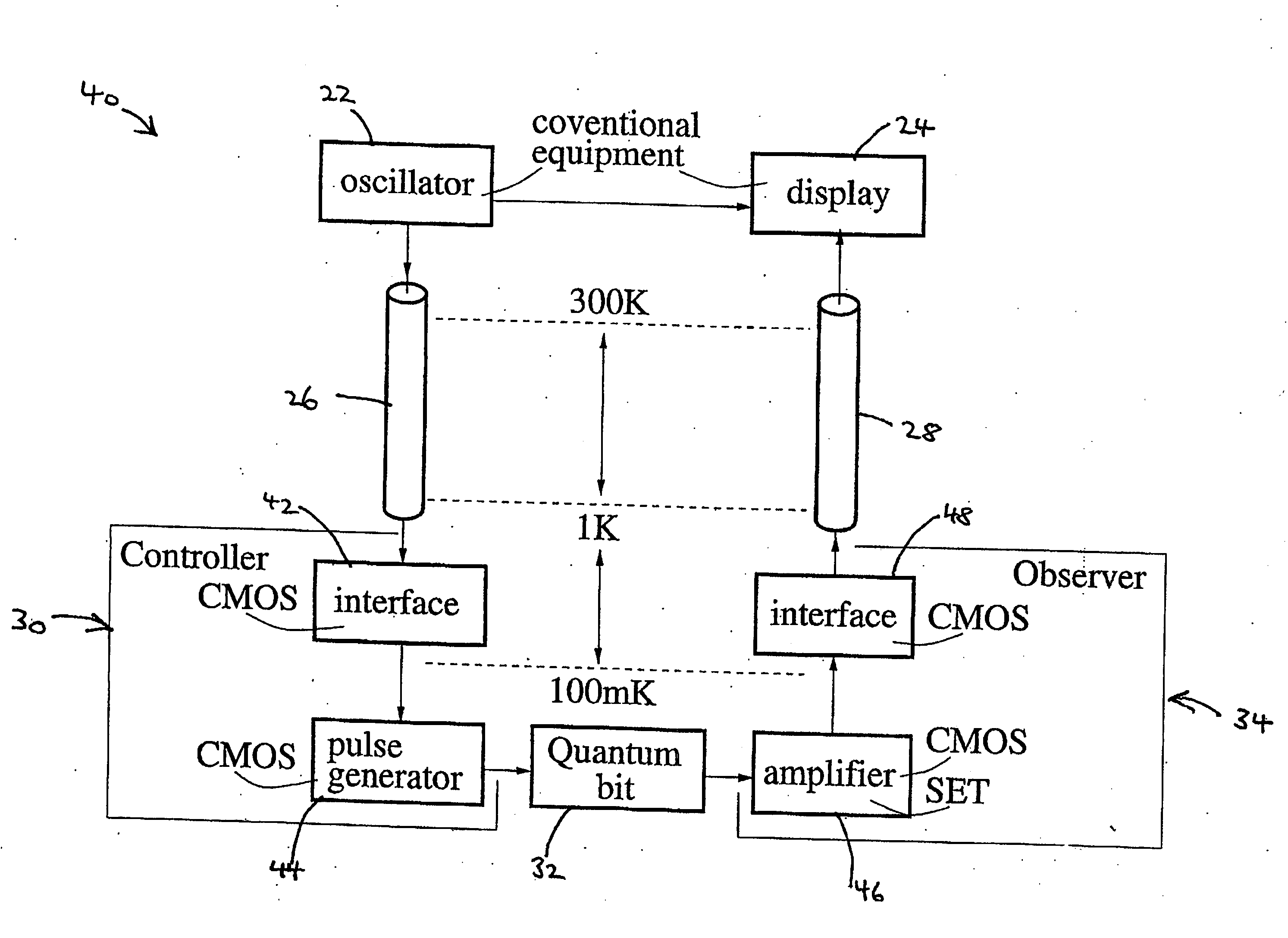
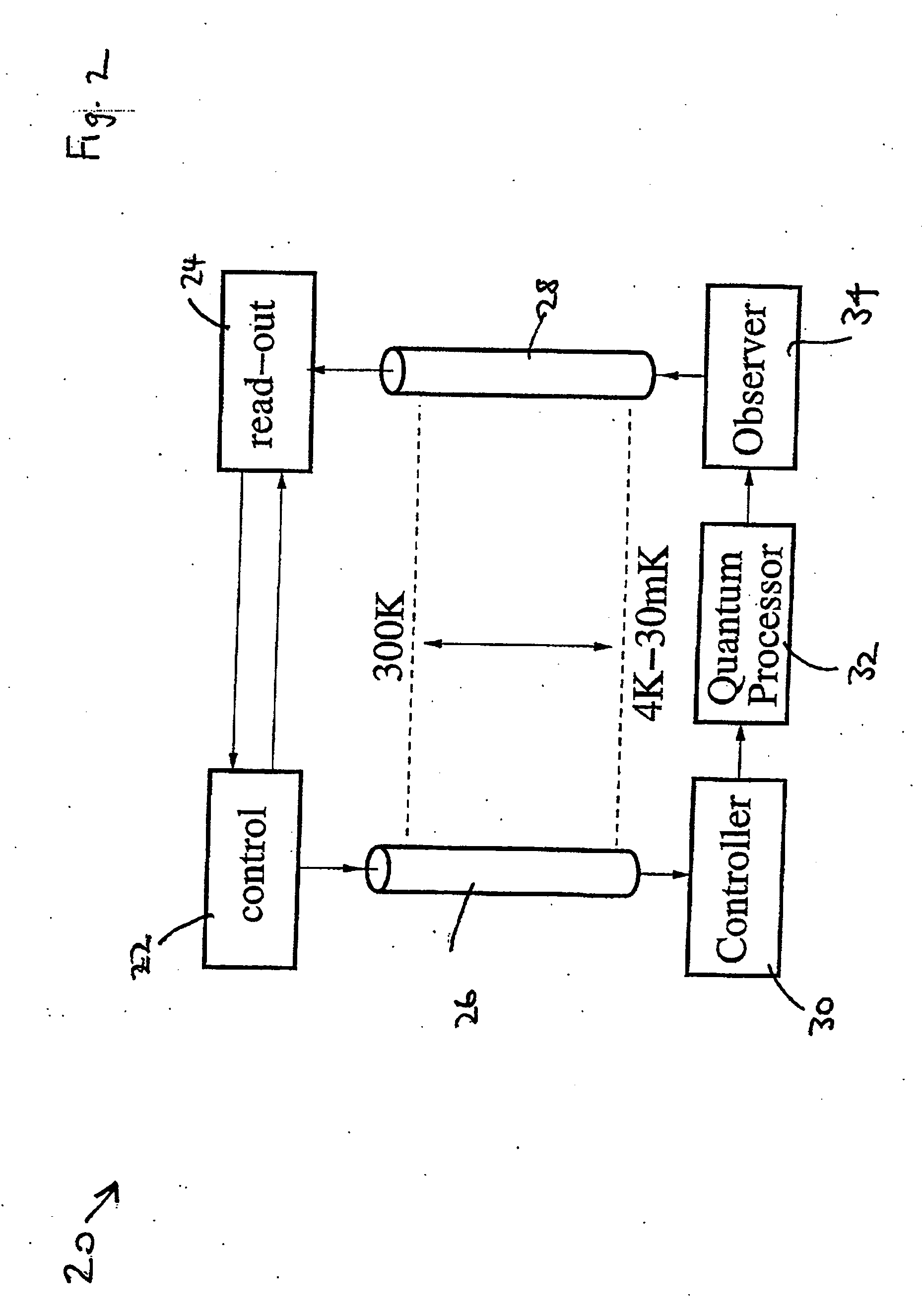
Interfacing at low temperature using CMOS technology
a low temperature, cmos technology, applied in the direction of pulse generators, instruments, pulse techniques, etc., can solve the problems of unsuitable use for control of quantum circuits, not usually practical to produce cmos circuits of even modest complexity in research laboratories, etc., to achieve convenient interface, high unity-gain frequency, and high temporal control
- Summary
- Abstract
- Description
- Claims
- Application Information
AI Technical Summary
Benefits of technology
Problems solved by technology
Method used
Image

Examples
Embodiment Construction
Part 1
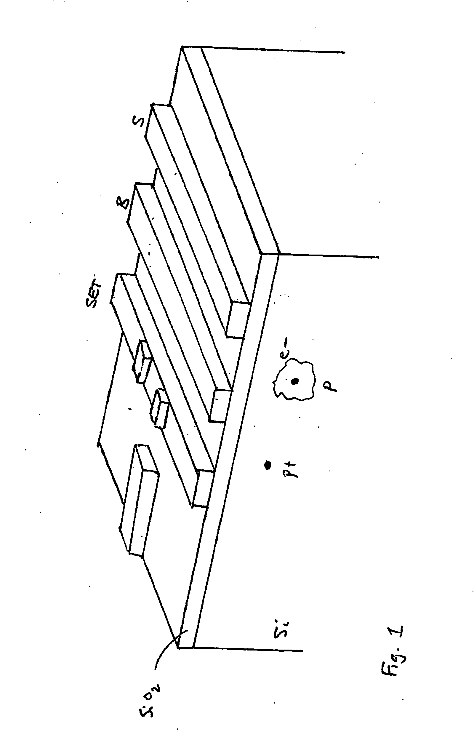
[0027]This example concerns the control and readout for a silicon (Si) based quantum computer. A quantum binary digit (qubit) is the fundamental computational element of the quantum computer. The solid-state qubit can be either a spin qubit [1], or a charge qubit [2]. In this example we consider a silicon charge qubit, however, we note that silicon spin-based qubits are expected to have much longer quantum coherence times and would be the preferred choice in most cases.
[0028]A buried donor charge qubit is shown in FIG. 1 for the case of P dopants in Si, although a number of other dopant-substrate systems could also be considered. The lowest two states of a single electron localized by the double well formed by two donor P+ ions give rise to a natural identification of the quantum logic states. External control over the barrier height and potential offset (or symmetry) is facilitated by B and S gates, respectively, placed about the buried (P-P+) system. With appropriate negativ...
PUM
 Abstract
Description
Claims
Application Information