Display device

a display device and active matrix technology, applied in the field of display devices, can solve problems such as brightness unevenness and brightness unevenness

Inactive Publication Date: 2008-12-04
SONY CORP
View PDF4 Cites 50 Cited by
  • Summary
  • Abstract
  • Description
  • Claims
  • Application Information

AI Technical Summary

Benefits of technology

[0029]On the other hand, even in this case, all of a p-type and n-type transistor pair serving as an inverter type for determining the start timing, and a p-type and n-type transistor pair serving as an inverter type for determining the end timing are disposed by being arrayed in a column in the longitudinal direction of laser beam irradiation, whereby there is an advantage wherein with any driving, a state can be secured in a sure manner in which the buffer transistors for determining the start timing and the buffer transistors for determining the end timing are disposed by being arrayed in a column in the longitudinal direction of laser beam irradiation.

Problems solved by technology

If the pulse signal itself supplied from the scan circuit has waveform blunting, and the waveform blunting thereof differs for each scanning line, there are caused irregularities between the correction periods, and brightness unevenness occurs.
The waveform blunting of the pulse signal itself supplied from the scan circuit affects all of the pixel circuits connected to scanning lines similarly, and accordingly, brightness unevenness due to the irregularities regarding the waveform blunting appears for each scanning line (i.e., linearly).
This point is readily recognized visibly as compared with random brightness unevenness in the case of the threshold and mobility of each pixel circuit within the pixel array unit fluctuating at random, which causes a critical problem.

Method used


Image

  • Display device
  • Display device
  • Display device

Examples


first embodiment

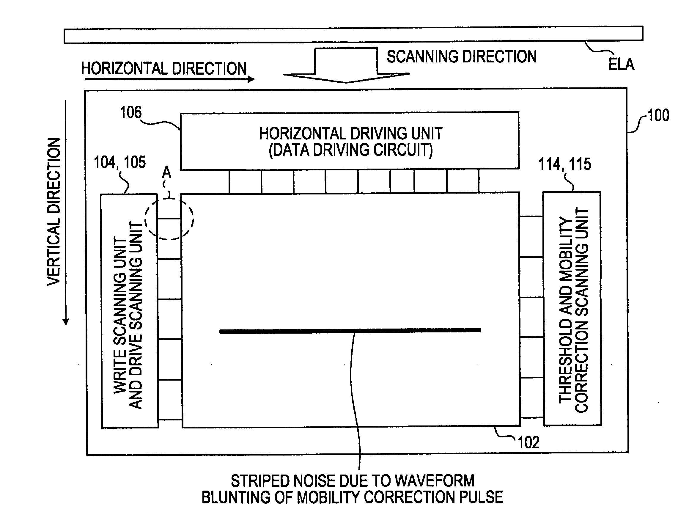
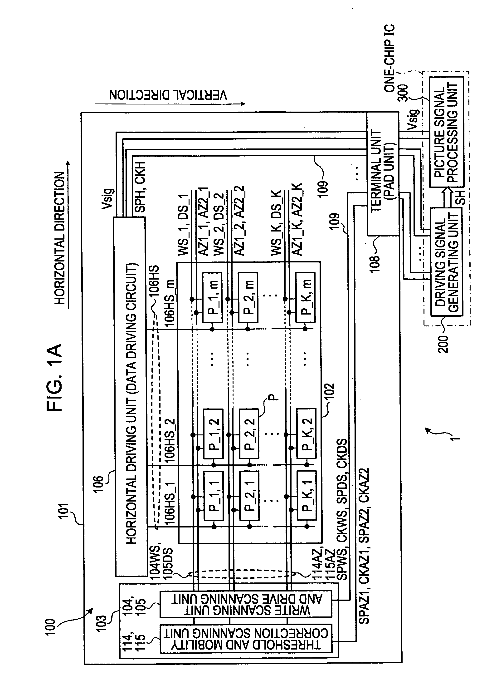
[0094]FIG. 2 is a diagram illustrating the pixel circuits P making up the organic EL display device 1 shown in FIGS. 1A and 1B. Note that FIG. 2 also illustrates the vertical driving unit 103 and horizontal driving unit 106 provided on the peripheral portion of the pixel circuits P on the substrate 101 of the display panel unit 100.

[0095]FIG. 3A is a diagram describing the operating points of the organic EL element and driving transistor. FIG. 3B is a diagram describing influence due to the property irregularities of the organic EL device and driving transistor given to a driving current Ids. FIG. 3C and FIG. 3D are diagrams describing the concept of improvement technique thereof.

[0096]The pixel circuits P according to the first embodiment shown in FIG. 2 have features in that a driving transistor is basically configured of an n-channel type thin film field-effect transistor, and also in that there are provided a circuit for suppressing fluctuation of the driving current Ids to the ...

second embodiment

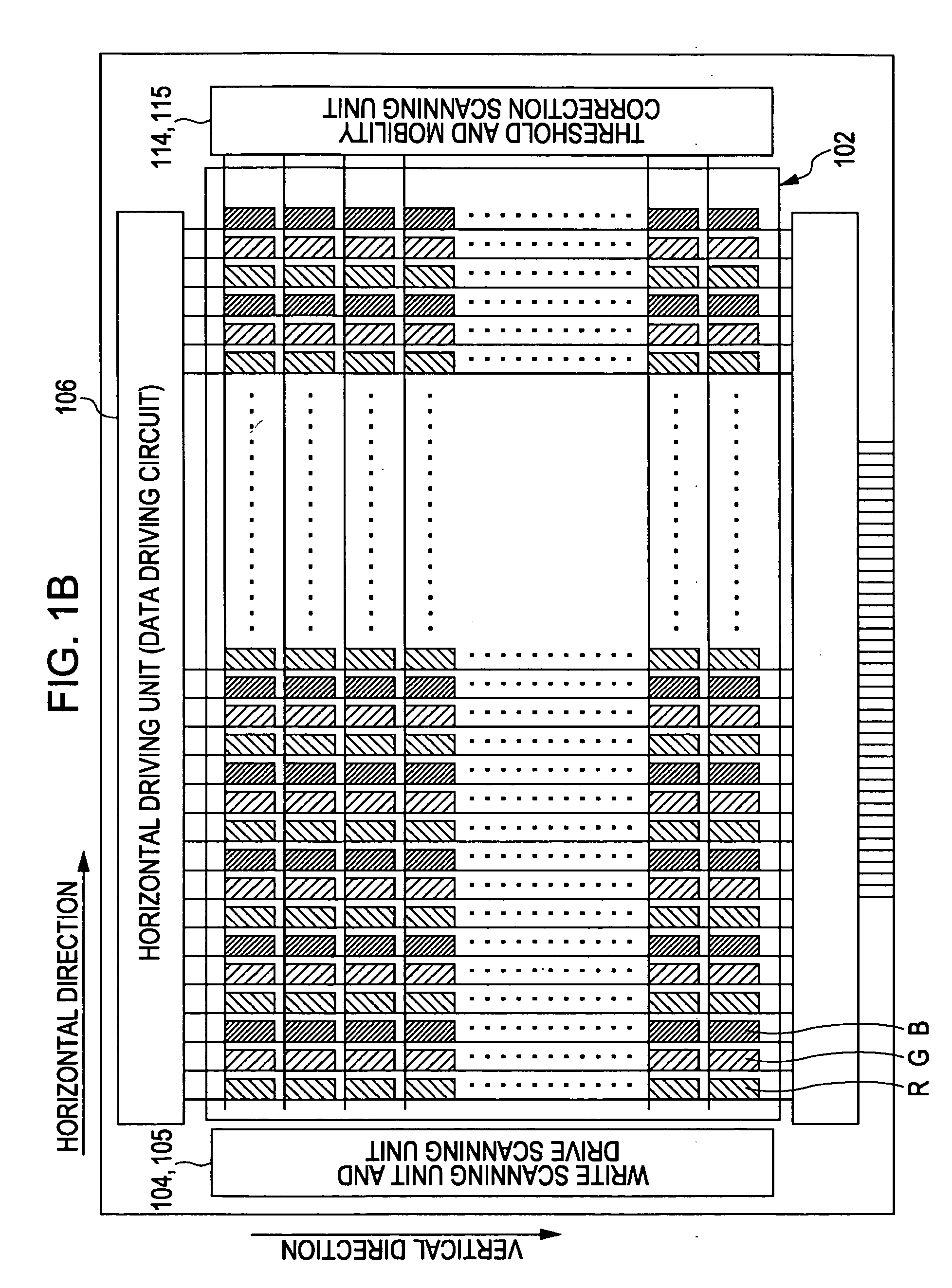
[0274]FIGS. 15A and 15B are diagrams illustrating the driving circuit placement (layout) whereby brightness irregularities on the display screen due to the irregularities cause at the time of the annealing processing can be alleviated.

[0275]A layout according to the second embodiment is an example wherein in the case of an operation period being determined with the ON period or OFF period of two transistors, the n-type light-emitting control transistor 122 and p-type sampling transistor 125 are included in the pixel circuit P as the two transistors. As for a driving timing example, as shown in FIG. 4, there is employed a case wherein upon the scan driving pulse NDS going to an active-low state during an active-high period of the write driving pulse WS, the mobility correction period starts, following which upon the write driving pulse WS going to an inactive-low state while the scan driving pulse NDS is kept in an active-low state, the mobility correction period ends.

[0276]The outpu...

third embodiment

[0282]FIGS. 17A and 17B are diagrams illustrating the driving circuit placement (layout) whereby brightness irregularities on the display screen due to the irregularities cause at the time of the annealing processing can be alleviated.

[0283]A layout according to the third embodiment corresponds to timing for driving the pixel circuit P according to the second embodiment shown in FIG. 16A and the pixel circuit P according to the second embodiment shown in FIG. 16B. That is to say, as shown in FIG. 16B, as for a driving timing example, there is employed a case wherein upon the scan driving pulse DS going to an active-high state during an active-high period of the write driving pulse WS, the mobility correction period starts, following which, upon the write driving pulse WS going to an inactive-low state while the scan driving pulse DS is kept in an active-high state, the mobility correction period ends.

[0284]The output circuit 400 is configured of the p-type transistor 402 and n-type ...


PUM


Abstract

A display device includes: a pixel array unit with pixel circuits disposed in matrix form, the pixel circuit including a driving transistor, an electro-optic element, a storage-capacitor, and a sampling transistor, with the electro-optic element emitting light by generating a driving current based on information stored in the storage-capacitor at the driving transistor to be applied to the electro-optic element; and a control unit, of which the output stage includes a buffer transistor, to output a pulse signal for driving the pixel array unit from the buffer transistor; wherein the pixel array unit and the control unit are formed with long laser beam irradiation to be scanned in the vertical direction; and with the control unit, buffer transistors for outputting a pulse signal for sampling to an input video signal to each signal line are arrayed in a column in the longitudinal direction of the laser beam irradiation.

Description

CROSS REFERENCES TO RELATED APPLICATIONS[0001]The present invention contains subject matter related to Japanese Patent Application JP 2007-068004 filed in the Japanese Patent Office on Mar. 16, 2007, the entire contents of which are incorporated herein by reference.BACKGROUND OF THE INVENTION[0002]1. Field of the Invention[0003]The present invention relates to a display device including a pixel array unit where pixel circuits (also referred to as pixels) including an electro-optic element (also referred to as a display element or light-emitting element) are arrayed in a matrix form. More particularly, the present invention relates to an active-matrix display device wherein pixel circuits including an electro-optic element of which the brightness changes depending on the magnitude of a driving signal as a display element are disposed in a matrix form, each pixel circuit has an active element, and display driving is performed in increments of pixel by the active element thereof.[0004]...

Claims


Application Information

Patent Timeline
Patent Type & Authority Applications(United States)
IPC IPC(8): G09G3/30
CPCG09G3/3266G09G2310/0262G09G2300/043G09G3/3291G09G2300/0426G09G2320/0233G09G2320/0223G09G2300/0861G09G2300/0842G09G3/3233G09G2300/0819G09G2320/043G09G2310/0291
Inventor YAMASHITA, JUNICHIUCHINO, KATSUHIDE
Owner SONY CORP
Why Eureka
Try Eureka