Electro-Optical Apparatus and a Circuit Bonding Detection Device and Detection Method Thereof

a detection device and circuit technology, applied in semiconductor/solid-state device testing/measurement, semiconductor/solid-state device details, instruments, etc., can solve the problems of increased occurrence of defective products and risk so as to reduce the overall cost, reduce the possibility of failure to be examined, and reduce the cost and difficulty of circuit assembly

Active Publication Date: 2008-12-18
AU OPTRONICS CORP
View PDF2 Cites 6 Cited by
  • Summary
  • Abstract
  • Description
  • Claims
  • Application Information

AI Technical Summary

Benefits of technology

[0008]It is another objective of the present invention to provide a circuit bonding detection device and a detection method thereof to reduce the cost and difficulty in circuit assembly.
[0009]It is another objective of the present inventi...

Problems solved by technology

As FIG. 1 shows, events such as over-stress or uneven thickness of a base 33 of the chip 30, often causes the conductive bump 31 to deform, and increases the occurr...

Method used


Image

  • Electro-Optical Apparatus and a Circuit Bonding Detection Device and Detection Method Thereof
  • Electro-Optical Apparatus and a Circuit Bonding Detection Device and Detection Method Thereof
  • Electro-Optical Apparatus and a Circuit Bonding Detection Device and Detection Method Thereof

Examples


first embodiment

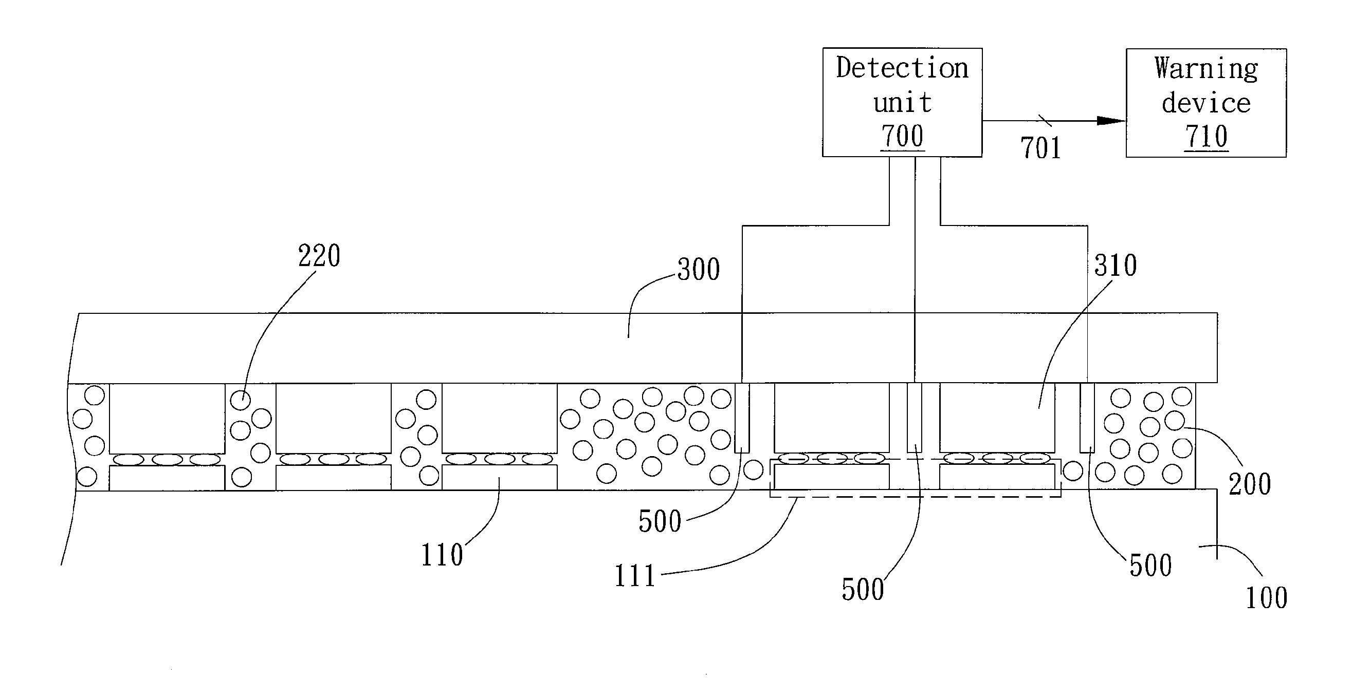
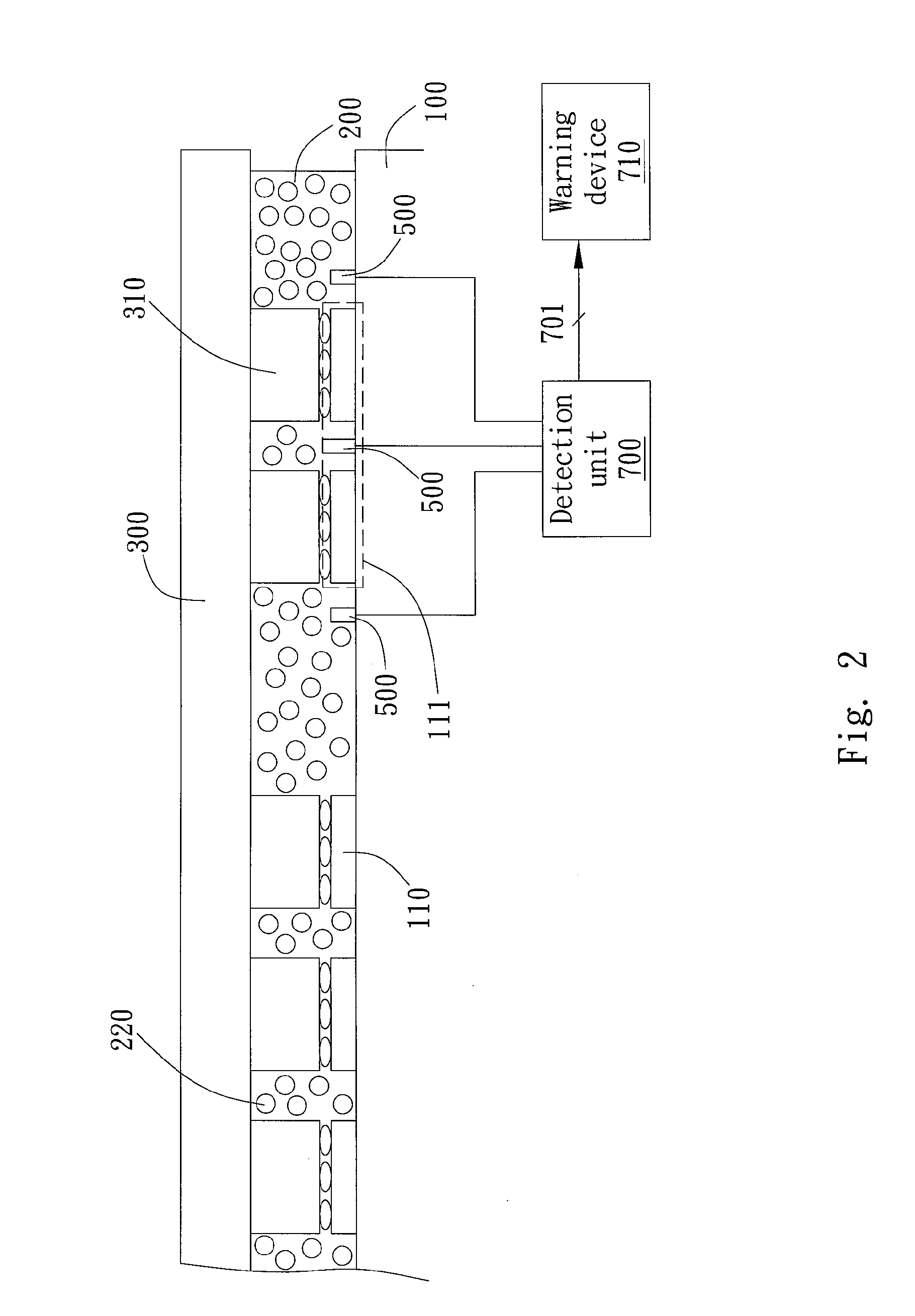
[0029]The circuit bonding detection device of the present invention includes a substrate 100, a circuit module 300, a set of sensors 500, and a detection unit 700. In the first embodiment shown in FIG. 2, a plurality of contact pads 110 is disposed on the substrate 100, the contact pads 110 can be arranged in patterns such as juxtaposed pattern, delta pattern, or other suitable patterns. Furthermore, as FIG. 2 shows, a first group 111 is formed by at least one contact pad 110. The contact pad 110 is electrically coupled with the TFTs (thin-film transistors) of the substrate 100 or is electrically coupled with other circuits used for signal transmission. The substrate 100 can be made of flexible materials (such as rubber, polyacetyl group, polyalcohol group, polyester group, thermosetting polymer, thermoplastic polymer, or other suitable polymers, or combinations thereof, opaque materials (such as silicon chip, ceramics, or other suitable materials), or transparent materials (such as...

second embodiment

[0034]In the second embodiment shown in FIG. 4a, all contact pads 110 disposed on the substrate 110, may further include a second group 112 formed by a plurality of contact pads 110. As for the present embodiment, the first group 111 includes at least two contact pads. However, in different embodiments, the first group 111 can include one or more contact pads 110, such as one, two, three, fourth, five, or six contact pads etc. As FIG. 4a shows, when the first group 111 includes two adjacent contact pads 110, three sensors 500 can be each disposed in the middle of the two contact pads 110 and on two sides of the first group 111 and thus three sensors 500 are disposed in the first group 111. However, in different embodiments, the first group 111 may have two sensors 500 disposed on two sides of each contact pads 110, and thus two independent sensors 500 will be disposed between the two adjacent contact pads 110.

[0035]Moreover, the contact pads 110 of the first group 111 are disposed a...

third embodiment

[0038]In the third embodiment shown in FIG. 5a, the first group 111 includes a single contact pad 110. One sensor 500 is disposed on two sides of the contact pad 110 respectively. The contact pad 110 of the first group 111 is disposed at the outside of the second group 112, but is not limited thereto. The sensors 500 can be disposed at the outside of the first group 111 having at least two contact pads 110. It is preferred for the first group 111 to be an alignment contact pad, a dummy contact pad, or contact pads not for signal transmission. The contact pads 110 of the second group 112 include the contact pad for signal transmission, alignment contact pad, dummy contact pad or contact pads not for signal transmission. Similarly, the conductive bumps 310 can be separated into a first group and a second group to electrically couple with the contact pads 110.

[0039]An embodiment shown in FIG. 5b is the variation of the third embodiment shown in FIG. 5a. In this variation embodiment, th...


PUM


Abstract

This invention provides a circuit bonding detection device, a detection method thereof and an electro-optical apparatus incorporating the circuit bonding detection device. The circuit bonding detection device includes a substrate, a circuit module, a set of sensors, and a detection unit. A plurality of contact pads is disposed on the substrate. The circuit module includes a plurality of conductive bumps corresponding to the contact pads. The sensors are disposed on two sides of at least one of contact pads or of the corresponding conductive bumps. The detection unit is electrically coupled with the set of sensors and transmits a fault signal when at least one of the contact pads and the corresponding conductive bumps deforms and contacts the sensors.

Description

BACKGROUND OF THE INVENTION[0001]1. Field of the Invention[0002]This present invention relates to a circuit bonding detection device, a detection method thereof and an electro-optical apparatus incorporating the circuit bonding detection device. More particularly, the present invention relates to a display panel circuit bonding detection device, detection method thereof and a display panel incorporating the display panel circuit bonding detection device and the detection method thereof.[0003]2. Description of the Prior Art[0004]The advance in display panel technology drives the demand for technology development in the packaging of display panel driver IC (Integrated Circuit). The conventional IC (Integrated Circuit) package method in the TFT-LCD (Thin-Film Transistor Liquid Crystal Display) includes TAP (Tape Carrier Package), COF (Chip On Film), and COG (Chip On Glass), wherein the package method of COG (Chip On Glass) has the advantages of lower cost, simplicity in manufacture pro...

Claims


Application Information

Patent Timeline
IPC IPC(8): H01L31/00
CPCH01L24/16H01L24/32H01L2924/01079H01L2924/14H05K1/0268H05K3/323H05K2201/10121H05K2203/162H05K2203/166H01L2924/10253H01L2924/00H01L2924/00011H01L2924/00014H01L2224/0401
Inventor TSAI, YING-HUNGCHOU, SHIH-PINGHUANG, CHING-YU
Owner AU OPTRONICS CORP
Why Eureka
Try Eureka