

Substrate-level assembly for an integrated device, manufacturing process thereof and related integrated device
- Summary
- Abstract
- Description
- Claims
- Application Information
AI Technical Summary
Benefits of technology
Problems solved by technology
Method used
Image

Examples
Embodiment Construction
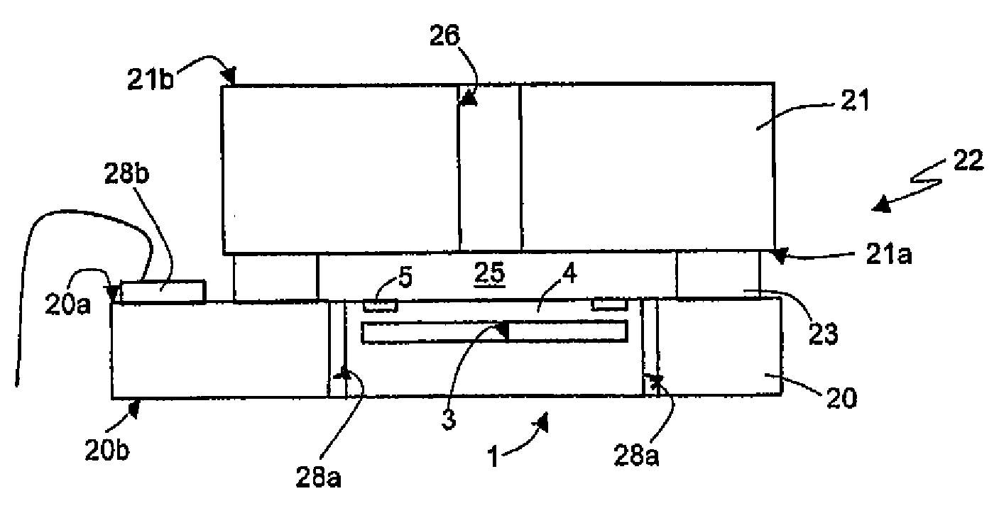
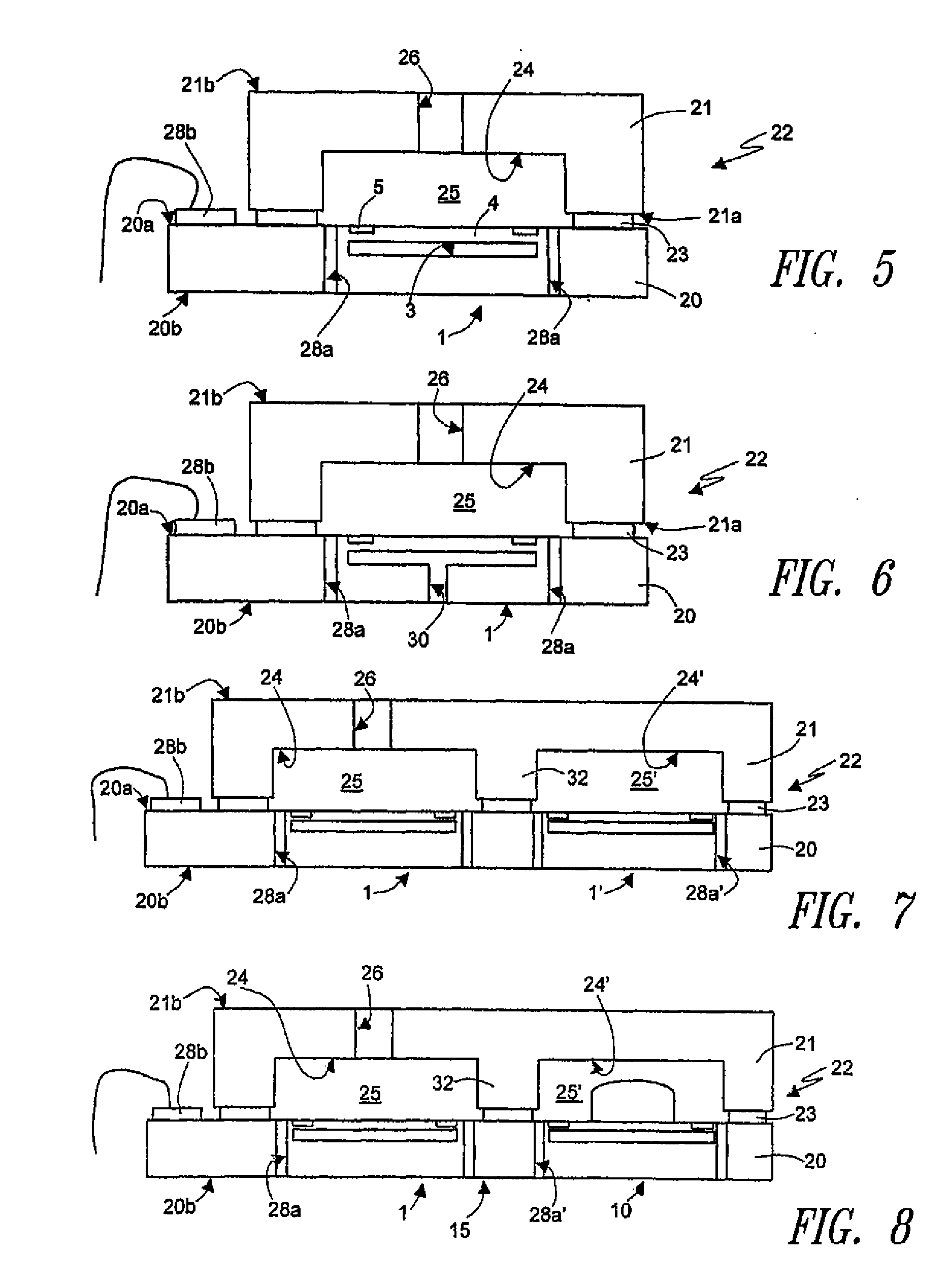
[0035]FIG. 5 shows a substrate 20 of semiconductor material, for example, monocrystalline silicon, having a top surface 20a and a bottom surface 20b, opposite to the top surface 20a (in what follows, the substrate 20 will be referred to as “device substrate,” in so far as it is designed to integrate one or more integrated devices, in particular, sensor devices).
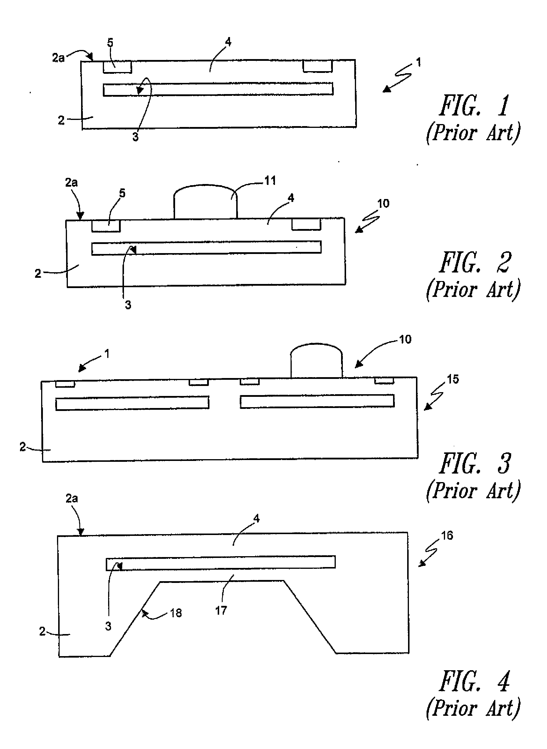
[0036]An integrated device, namely a pressure sensor 1, is formed inside the device substrate 20, as described with reference to FIG. 1 (so that parts that are similar are designated by the same reference numbers). In particular, the membrane 4, suspended over the buried cavity 3, is formed at the top surface 20a of the device substrate 20.
[0037]According to an aspect of the present disclosure, a capping substrate 21, made of semiconductor material (for example, silicon), glass, or other ceramic or polymeric material, is (mechanically or electrically or a combination of mechanically and electrically) coupled to the device sub...
PUM
 Abstract
Description
Claims
Application Information