

Packaged electronic modules and fabrication methods thereof implementing a cell phone or other electronic system
a cell phone or other electronic system and electronic module technology, applied in the direction of printed circuit manufacturing, printed circuit aspects, cross-talk/noise/interference reduction, etc., can solve the problems of speed, and the conventional limit of process speed, and achieve the goal of providing electronic packaging and interconnects which provide maximum performance. , the problem of speed and size and interconnect density
- Summary
- Abstract
- Description
- Claims
- Application Information
AI Technical Summary
Benefits of technology
Problems solved by technology
Method used
Image

Examples
Embodiment Construction
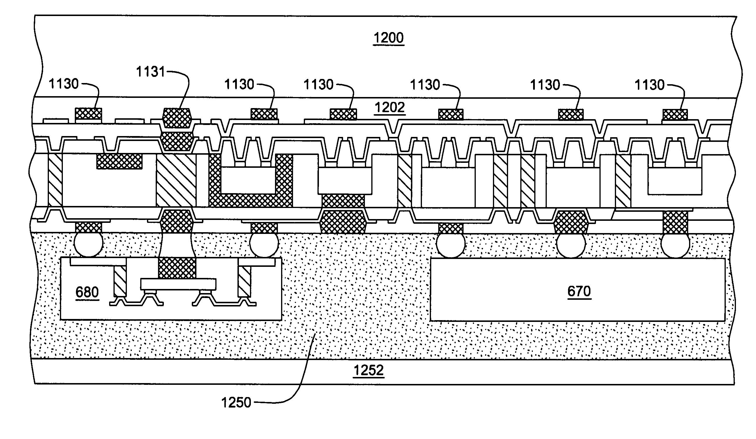
[0028]Generally stated, provided herein are numerous enhancements to multichip modules, and in particular, to chips-first multichip modules. Advantageously, complete electronic systems or subsystems, and methods of fabrication thereof are disclosed herein in which a second layer of modules or other circuit components is connected to a multichip layer fabricated as a chips-first module. The multichip layer forms a base for the second layer of modules or components. Structures are provided for making through connection from a front surface to a back surface of the multichip layer. Interconnect structures are provided over the front surface of the multichip layer for interconnecting contact pads of integrated circuit chips in the multichip layer, as well as for connecting second layer components or for connecting to input / output contacts. The multichip modules disclosed herein include input / output contacts (e.g., contact pads or bumps) which may be placed at any location above the fron...
PUM
| Property | Measurement | Unit |
|---|---|---|
| size | aaaaa | aaaaa |
| thickness | aaaaa | aaaaa |
| thickness | aaaaa | aaaaa |
Abstract
Description
Claims
Application Information