Display Device

a technology of a display device and a display device, which is applied in the direction of cathode ray tubes/electron beam tubes, electrical discharge tubes, electrical apparatus, etc., can solve the problems of coil spring contact with the anode, coil deterioration, and the connection is not reliable, so as to prevent the deterioration of the withstand voltage characteristics, high voltage, and high reliability

Inactive Publication Date: 2008-12-25
HITACHI LTD
View PDF4 Cites 11 Cited by
  • Summary
  • Abstract
  • Description
  • Claims
  • Application Information

AI Technical Summary

Benefits of technology

[0013]According to still another aspect of the present invention, a thin plate of a metal with a thermal expansion coefficient close to the glass is used for the anode terminal. According to a first embodiment of the present invention, a thin plate of an Fe—Ni alloy with a thermal expansion coefficient matched to the glass is used for the anode terminal. Thus, there is no possibility that the contact spring is bonded to the glass. As a result, it is possible to supply a high voltage to the anode substrate with a high reliability.
[0014]According to still another aspect of the present invention, the shape of the contact spring and its surface roughness are determined by specific values, in order to prevent deterioration of the withstand voltage characteristics due to the contact spring.
[0015]According to still another aspect of the present invention, the contact spring is applied with a high voltage. The relationship between the contact spring and an internal component of an FED is determined by a specific value, in order to reduce the possibility of a spark.
[0016]According to still another aspect of the present invention, the shape of the anode electrode formed in the anode substrate, namely, the metal back is defined in an appropriate manner, in order to reduce the possibility of a spark due to the anode substrate.
[0017]According to the present invention, the contact spring is used for supplying a high voltage, so that it is possible to supply the high voltage to the anode substrate with a high reliability. Also, according to the present invention, it is possible to sufficiently maintain the air tightness with the glass plate in the high voltage introduction terminal portion.
[0018]Further, according to the present invention, it is possible to ensure the reliability of the anode terminal of the anode substrate that the contact spring contacts. Still further, according to the present invention, it is possible to prevent a spark from occurring between the parts including the contact spring used in the high voltage introduction portion, or between the structures.

Problems solved by technology

In the case of a coil spring, there remains a problem with the reliability of the connection between the coil spring and the high voltage introduction terminal, or the contact between the coil spring and the anode.
The use of the coil spring has another problem that when a large current flows through the coil spring, the coil is reduced by electromagnetic force, preventing the contact between the anode and the coil spring.
While the use of a plate-like spring has a problem of instability of the contact between an end of the plate spring and a voltage supply terminal of the anode substrate.
In other words, in the case of a typical plate spring, the contact between the anode terminal and the plate spring is a point contact, causing a problem of conduction failure as a result of repeating ON and OFF operation.
The coil spring or the plate spring and the like should contact the anode substrate, posing a problem of instability in the contact portion.
There is another problem that a spark occurs due to the shape of parts in the vicinity of a terminal for introducing a high voltage, or other factors.

Method used


Image

  • Display Device
  • Display Device
  • Display Device

Examples


first example

First Embodiment

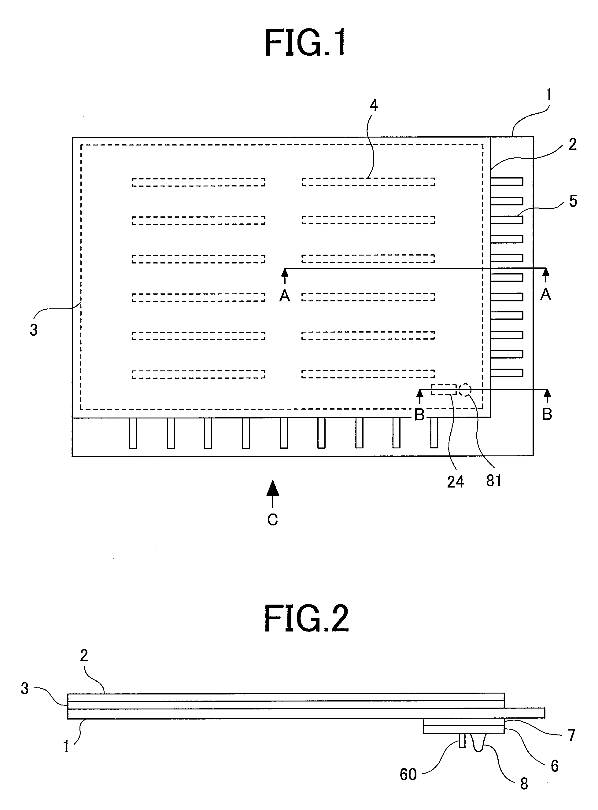
[0079]FIG. 1 is a plan view showing an FED to which the present invention is applied. In FIG. 1, an anode substrate 2 is provided above a cathode substrate 1 through a sealing portion 3. On the cathode substrate there are provided scan lines extending in the horizontal direction, as well as data signal lines extending in the vertical direction. The scan lines and the data signal lines are supplied with signals from the outside through terminals 5. Electron emission sources are provided in the vicinity of the intersections of the scan lines and the signal lines. In other words, a large number of electron emission sources are arranged in a matrix form. Various types of electron emission source have been developed, such as so-called MIM-type, SID-type, and Spindt-type, all of which can be applied to the embodiment.

[0080]The interior, which is defined by the cathode substrate 1, the anode substrate 2, and the surrounding sealing portion 3, is maintained at a vacuum. In s...

forth embodiment

[0115]FIG. 25 is a schematic cross-sectional view showing a forth embodiment the present example. In FIG. 25, the high voltage introduction terminal 60 is formed passing through the cathode substrate 1 while maintaining air tightness against the outside. In the present embodiment, the exhaust tube 8 is also attached to the cathode substrate 1 directly by the frit glass, and not through the exhaust plate 6. FIG. 25 shows the state in which the exhaust tube 8 is chipped off.

[0116]In the present embodiment, the configuration is the same as described in the third embodiment in FIG. 20, except that the exhaust tube 8 is attached to the cathode substrate 1 and not to the exhaust plate 6. In the present embodiment, the high voltage introduction terminal 60 is attached to the cathode substrate 1 in advance. Thus, it is necessary to pay attention to the handling of the cathode substrate 1. Meanwhile, it is possible to omit the process of sealing the exhaust plate 6.

[0117]In FIG. 25, the cont...

second example

First Embodiment

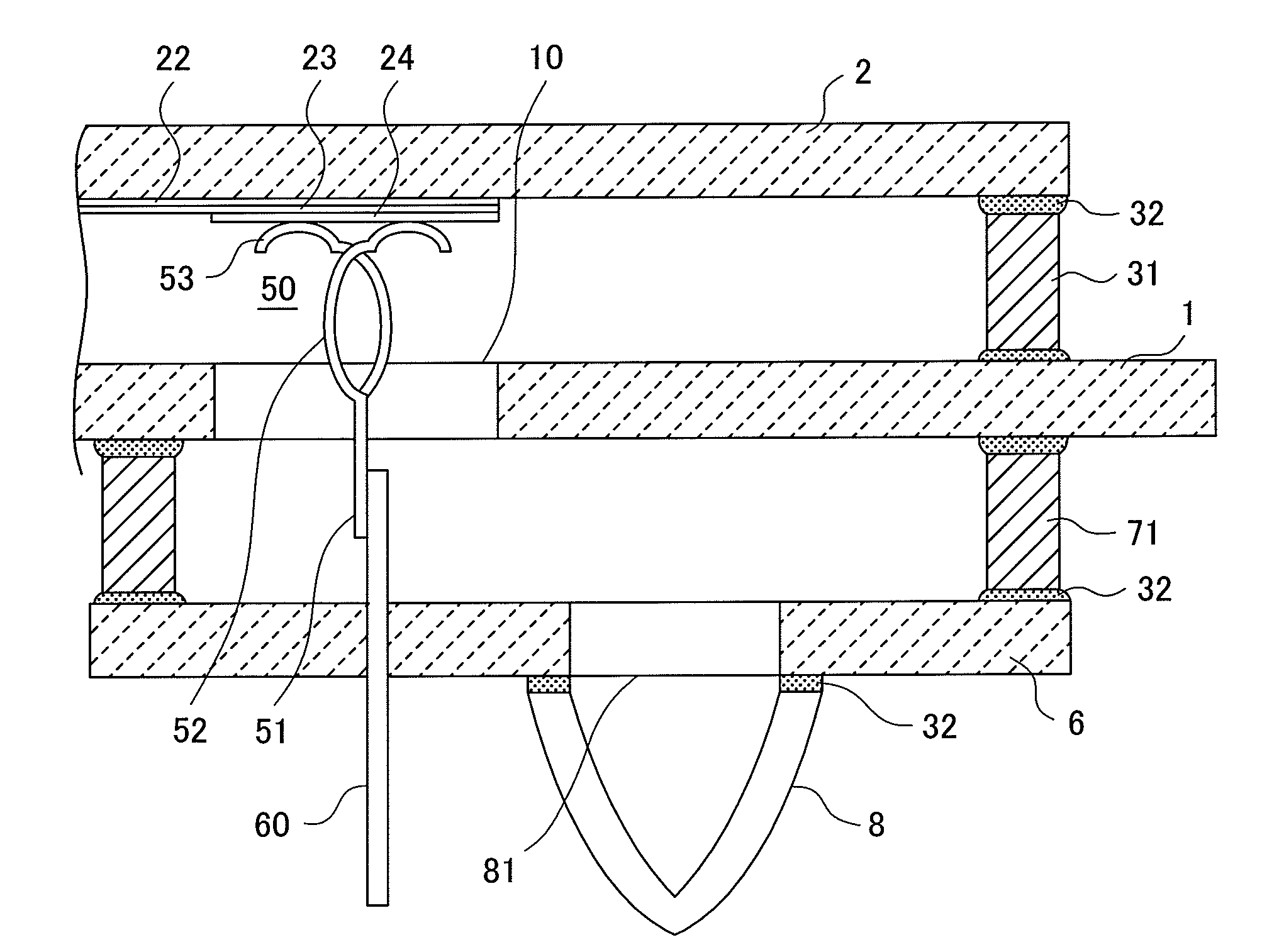
[0119]FIG. 26 is a B-B cross-sectional view of FIG. 1, which shows a substantial portion of a first embodiment. In FIG. 26, the through hole 10 is formed in the cathode substrate 1. The evacuation of the display device, or the high voltage supply is performed through the through hole 10. The exhaust plate 6 is provided covering the through hole 10 of the cathode substrate 1 through the exhaust plate sealing portion 7. In this way, the interior of the display device is maintained at a vacuum. The basic configuration of the exhaust plate sealing portion 7 is the same as that of the sealing portion 3 for sealing the cathode substrate 1 and the anode substrate 2. In other words, the exhaust plate frame 71 is sealed to the cathode substrate 1 and to the anode substrate 2 through the sealing 32. In the present embodiment, the thickness of the frame 31 for sealing the anode substrate 2 and the cathode substrate 1, and the thickness of the frame for sealing the cathode subst...


PUM


Abstract

There is disclosed an FED (field emission display) capable of supplying an anode voltage, which is a high voltage, to an anode substrate with high reliability. A high voltage introduction button is sealed to a sealing plate, in which a contact spring is attached to the high voltage introduction button by spot welding. The high voltage introduction button has a flat portion connected to the contact spring, a sealing portion sealed to the glass substrate, and an external terminal to be connected to an external power source. The contact spring contacts an anode terminal of an anode substrate with an appropriate contact pressure, by a spring force from an arm portion of the contact spring. The anode terminal is formed of a conductive film containing metal particles.

Description

CLAIM OF PRIORITY[0001]The present application claims priority from Japanese Application JP 2007-091764 filed on Mar. 30, 2007, Japanese Application JP 2007-124934 filed on May 9, 2007, Japanese Application JP 2007-124837 filed on May 9, 2007, Japanese Application JP 2007-222488 filed on Aug. 29, 2007, Japanese Application JP 2007-226308 filed on Aug. 31, 2007, the content of which is hereby incorporated by references into this application.FIELD OF THE INVENTION[0002]The present invention relates to a display device, and more particularly, to a flat display device having an interior maintained at a vacuum, including a rear substrate with electron emission sources arranged in a matrix form, and a front substrate with phosphors arranged in a corresponding manner.BACKGROUND OF THE INVENTION[0003]A field emission display (FED) having an interior that is defined between two glass substrates and maintained at a vacuum, in which electron emission sources are arranged on one substrate in a ...

Claims


Application Information

Patent Timeline
Patent Type & Authority Applications(United States)
IPC IPC(8): H01J29/90
CPCH01J29/90H01J29/925H01J29/94H01J31/123H01J2329/90H01J2329/92H01J2329/941
Inventor KITADA, TAKAAKINAITO, TAKASHIHIRASAWA, SHIGEMIHATORI, AKIRASHIRAI, SHOJIASAKURA, SHUNICHIYANO, MAKOTOKIJIMA, YUUICHIHOSOTANI, NOBUHIKOSAITO, GO
Owner HITACHI LTD
Why Eureka
Try Eureka