Method for manufacturing semiconductor package
- Summary
- Abstract
- Description
- Claims
- Application Information
AI Technical Summary
Benefits of technology
Problems solved by technology
Method used
Image


Examples
Embodiment Construction
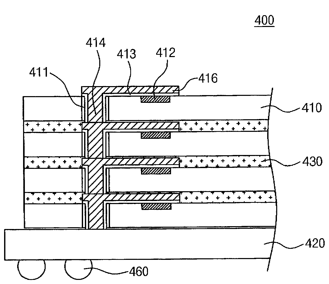
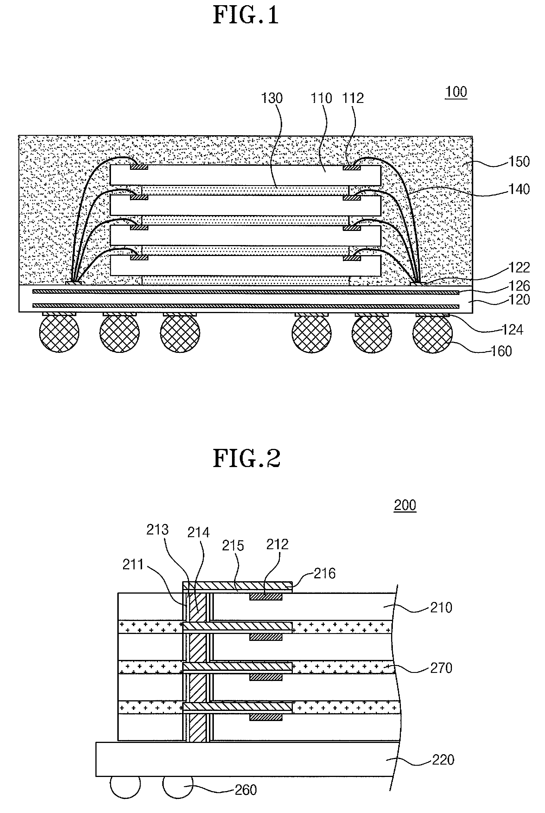
[0042]A preferred embodiment of the present invention is directed to a method for manufacturing a semiconductor package in which a through silicon via and a redistribution layer, connecting the through silicon via to a bonding pad, are formed simultaneously. Further, a preferred embodiment of the present invention is directed to a method for manufacturing a semiconductor package in which semiconductor chips are stacked vertically such that mold parts are formed on both upper and lower surfaces of the semiconductor chip formed with the through silicon via and the redistribution layer.
[0043]Therefore, in an embodiment of the present invention, since the through silicon via and the redistribution layer are formed not separately but simultaneously, it is possible to simplify the process and reduce manufacturing costs.
[0044]Also, in an embodiment of the present invention, because the stack type semiconductor package is realized by stacking the semiconductor chips formed with the mold par...
PUM
 Abstract
Description
Claims
Application Information