Substrate processing apparatus and semiconductor device manufacturing method

a processing apparatus and semiconductor technology, applied in the direction of liquid surface applicators, coatings, chemical vapor deposition coatings, etc., can solve the problems of foreign matter contamination of substrates, inability to easily flow cleaning gas, and inability to clean up

Inactive Publication Date: 2009-01-01
KOKUSA ELECTRIC CO LTD
View PDF7 Cites 21 Cited by
  • Summary
  • Abstract
  • Description
  • Claims
  • Application Information

AI Technical Summary

Benefits of technology

[0036]the control section controls the exhaust valve, the third gas supply valve and the fourth gas supply valve to alternatively supply the first raw material gas and the second raw material gas when the first raw material gas and the second raw material gas are supplied to form a desired film on the substrate,

Problems solved by technology

In this case, there is a possibility that the accretions cause foreign matter contamination of a substrate.
At these times, it is conceived that impurities or accretions including the impurities float in the processing chamber or a member (e.g., a gas supply tube) which is in communication with the processing chamber, and this causes foreign matter contamination.
According to the method using the above-mentioned self cleaning, however, a region where the cleaning gas can not flow easily (dead space) is formed in th

Method used


Image

  • Substrate processing apparatus and semiconductor device manufacturing method
  • Substrate processing apparatus and semiconductor device manufacturing method
  • Substrate processing apparatus and semiconductor device manufacturing method

Examples


Embodiment Construction

[0067]Next, preferred embodiments of the present invention will be explained with reference to the drawings.

[0068]A substrate processing apparatus according the present embodiment is constituted as a semiconductor device manufacturing apparatus, as one example, which is used for manufacturing a semiconductor device integrated circuit (IC). In the following description, a case in which a vertical type apparatus which subjects a substrate to a thermal processing and the like and which is used as one example of the substrate processing apparatus will be described.

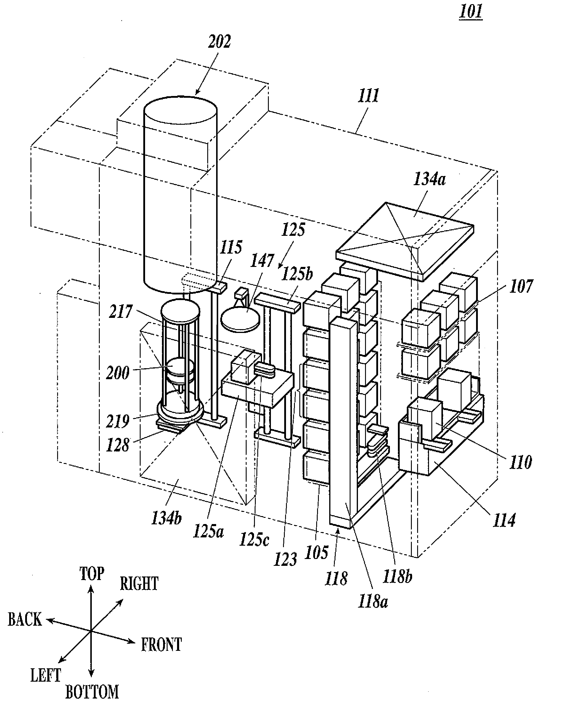
[0069]As shown in FIG. 1, a processing apparatus 101 uses cassettes 110 which accommodate wafers 200, which are one example of the substrate. The wafers 200 are made of a material such as silicon. The substrate processing apparatus 101 includes a casing 111 and a cassette stage is disposed inside the casing 111. The cassette 110 is transferred onto the cassette stage 114 and carried out from the cassette stage 114 by a transpo...


PUM

PropertyMeasurementUnit
Pressureaaaaaaaaaa
Pressureaaaaaaaaaa
Chemical formulaaaaaaaaaaa

Abstract

Disclosed is a substrate processing apparatus which includes: a processing chamber to process a substrate; an exhaust path to exhaust the processing chamber; an exhaust device; an exhaust valve to open and close the exhaust path; a raw material gas supply member to supply raw material gas which contributes to film forming into the processing chamber; a cleaning gas supply member to supply cleaning gas which removes an accretion which adheres to an inside of the processing chamber with the raw material gas being supplied, the cleaning gas supply member comprising a supply path to supply the cleaning gas to the processing chamber and a supply valve to open and close the supply path; and a control section which controls the exhaust valve and the supply valve to supply the cleaning gas from the supply path to the processing chamber with exhaustion of the processing chamber being stopped.

Description

BACKGROUND OF THE INVENTION[0001]1. Field of the Invention[0002]The present invention relates to a substrate processing apparatus and a semiconductor device manufacturing method, and more particularly, to a substrate processing apparatus and a semiconductor device manufacturing method which supply raw material gas, which is to form a desired film, onto a substrate surface to form the desired film on the substrate surface.[0003]2. Description of the Related Art[0004]In the substrate processing apparatus of this kind, when raw material gas is supplied, the raw material gas flows also to other portions (e.g., an inner wall of a processing chamber) in addition to a surface of the substrate, and an unnecessary film is accumulatively deposited as accretions. Impurities, which are not harmless to substrate processing, may be mixed in the accretions. In this case, there is a possibility that the accretions cause foreign matter contamination of a substrate.[0005]That is, if the accretions ar...

Claims


Application Information

Patent Timeline
IPC IPC(8): B05C11/00H01L21/30
CPCC23C16/4405H01L21/67109H01L21/3185C23C16/4412H01L21/0217
Inventor ASAI, MASAYUKI
Owner KOKUSA ELECTRIC CO LTD
Why Eureka
Try Eureka