

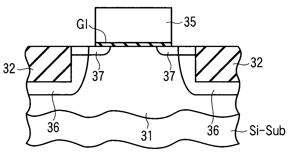
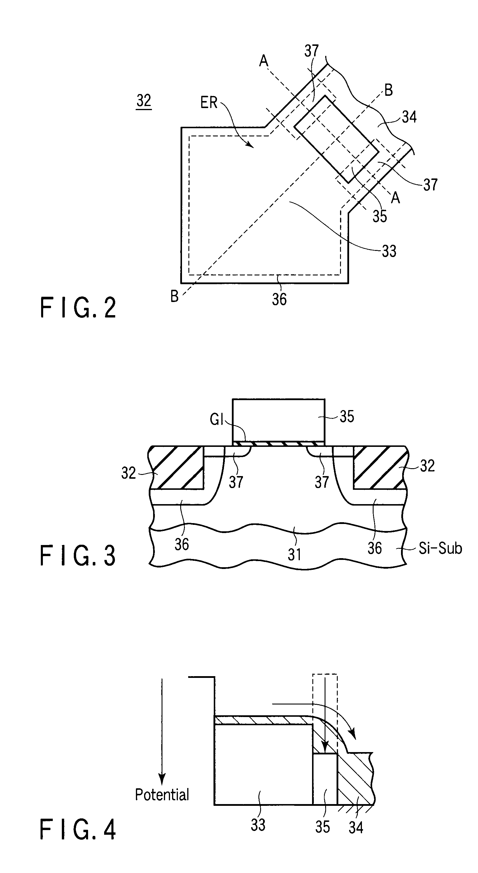
Solid-state imaging device with improved charge transfer efficiency
a solid-state imaging and efficiency-enhancing technology, applied in the direction of color television, television system, radio control device, etc., can solve the problems of many defects in the si semiconductor substrate, the afterimage of a reproduced image cannot be efficiently transferred by the transfer gate, and the defect of the image is not clear
- Summary
- Abstract
- Description
- Claims
- Application Information
AI Technical Summary
Problems solved by technology
Method used
Image

Examples
Embodiment Construction
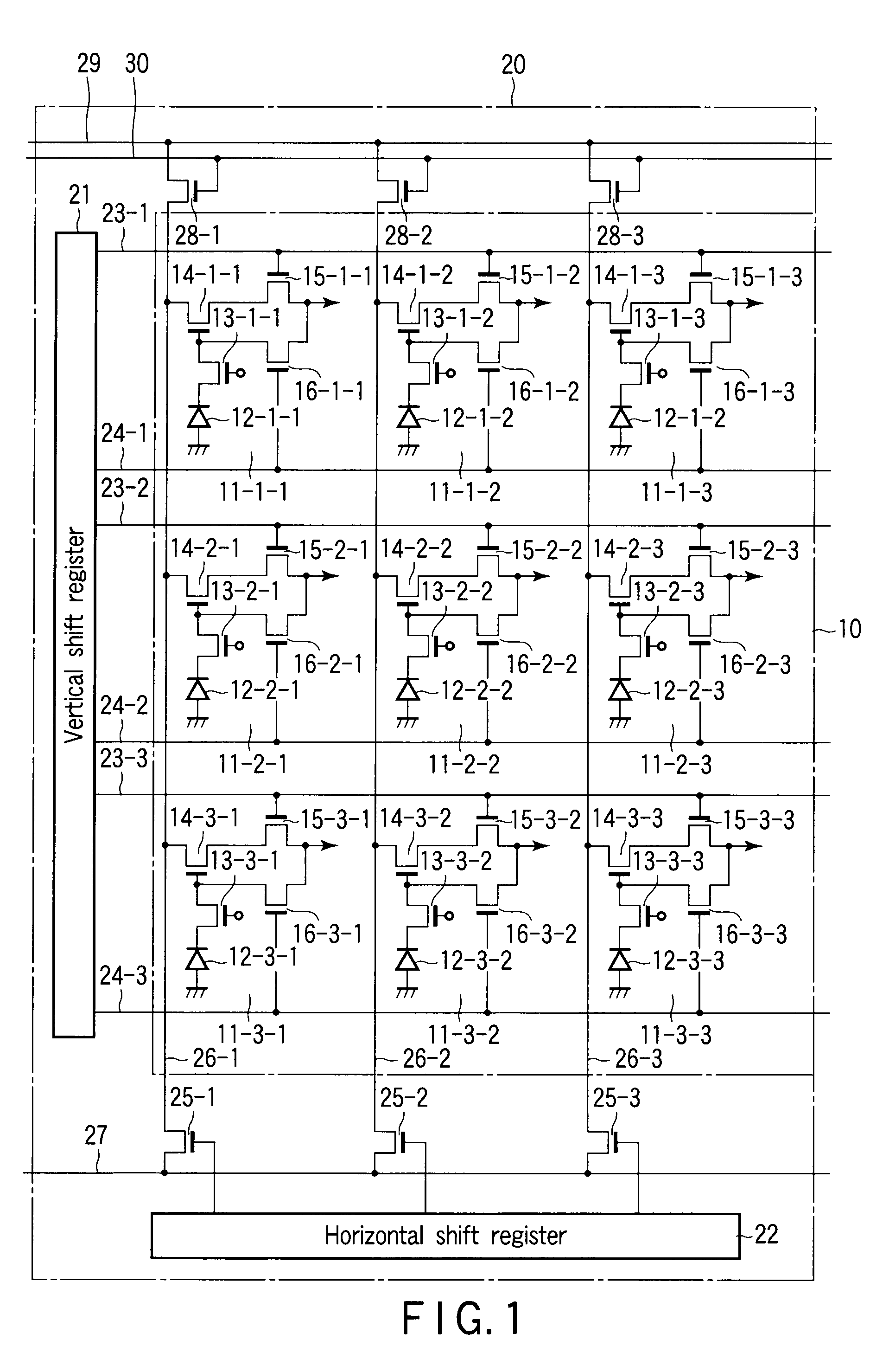
[0020]FIG. 1 is a circuit diagram showing the structure of the entirety of a pixel array in a solid-state imaging device according to an embodiment of the present invention. In FIG. 1, reference numeral 10 denotes a pixel region that is an imaging region, and numeral 20 denotes a peripheral circuit region. In the pixel region 10, a plurality of unit pixels (unit cells) 11 are arrayed in a two-dimensional fashion.
[0021]For the purpose of simple depiction, FIG. 1 shows, for example, unit cells 11-1-1 to 11-3-3 of three rows X three columns. Further, in the pixel region 10, there are provided horizontal address lines 23-1 to 23-3, reset lines 24-1 to 24-3 and vertical signal lines 26-1 to 26-3.
[0022]In the peripheral circuit region 20, there are provided a vertical shift register 21 which scans the pixel region 10, a horizontal shift register 22, vertical signal lines 26-1 to 26-3, load transistors 28-1 to 28-3, horizontal select transistors 25-1 to 25-3, and a horizontal signal line 2...
PUM
 Abstract
Description
Claims
Application Information