

Semiconductor device
a technology of semiconductor devices and shielding devices, applied in semiconductor devices, semiconductor/solid-state device details, electrical devices, etc., can solve problems such as particularly serious problems, and achieve the effects of preventing leakage, preventing leakage current and withstand voltage deterioration, and enhancing the effect of channel stoppers
- Summary
- Abstract
- Description
- Claims
- Application Information
AI Technical Summary
Benefits of technology
Problems solved by technology
Method used
Image

Examples
first embodiment
[0033]Embodiments of the present invention will be described in detail by reference to the drawings.
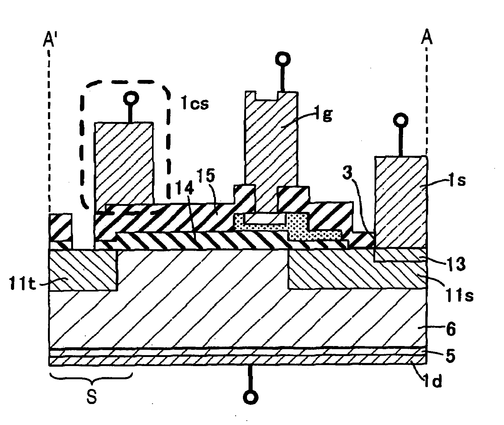
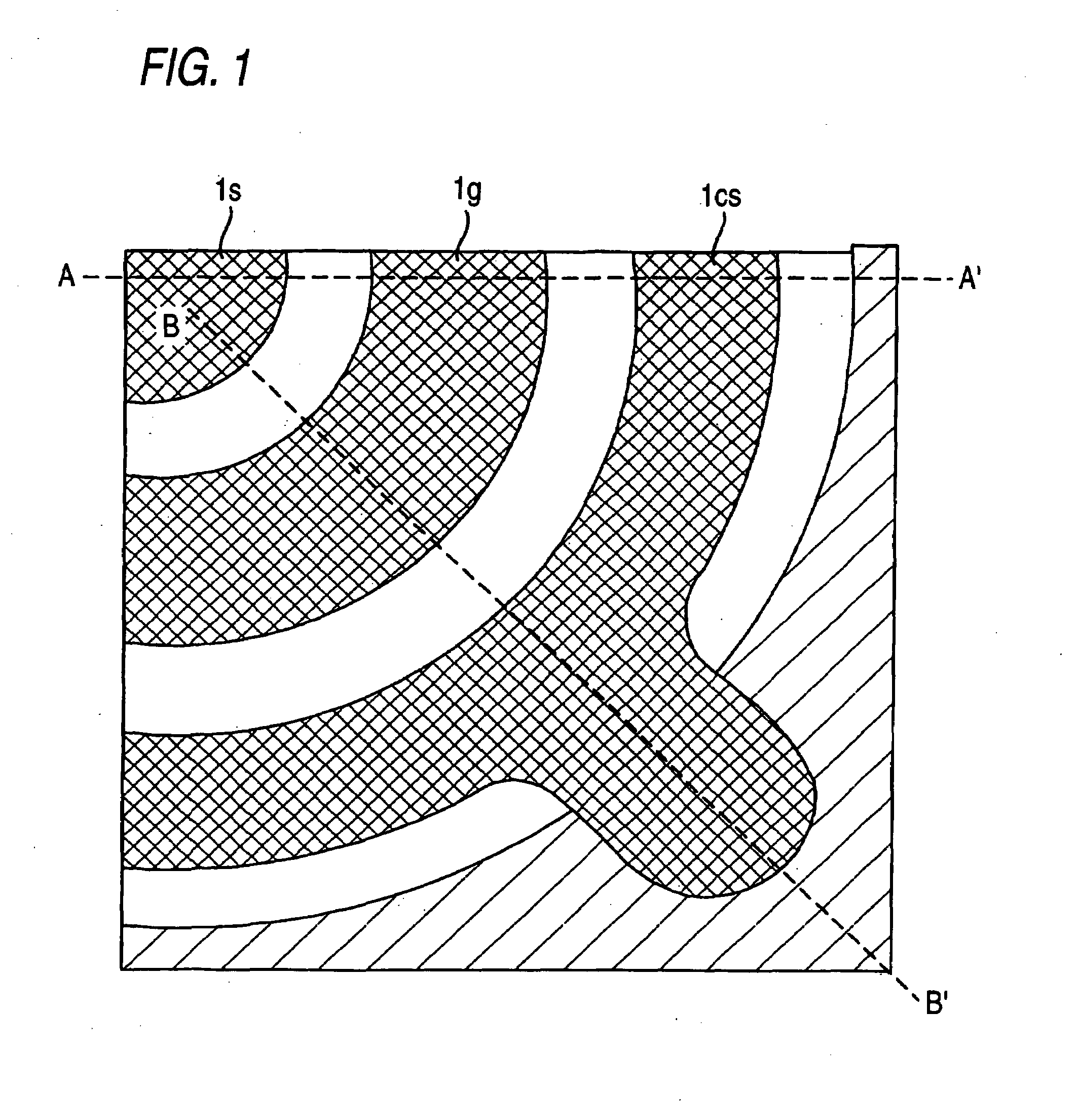
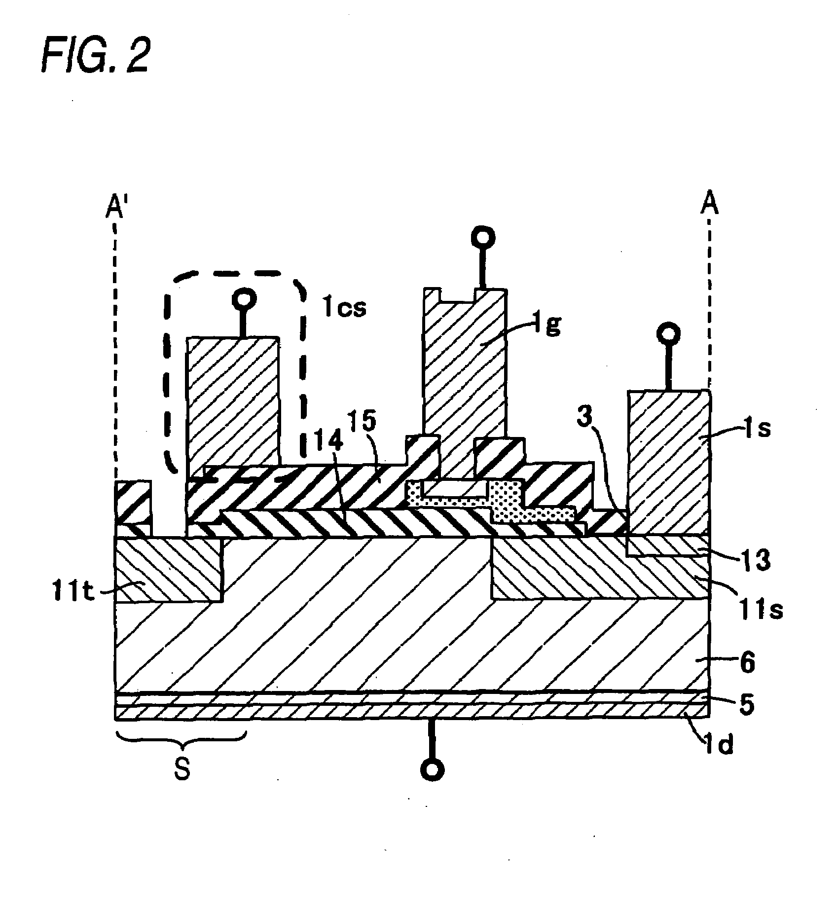
[0034]FIG. 1 is a conceptual plan view of a characteristic portion of a trench MOSFET of an embodiment of the present invention; FIG. 2 is a cross-sectional view taken along line A-A′ shown in FIG. 1; FIG. 3 is a cross-sectional view taken along line B-B′ shown in FIG. 1; FIGS. 4 and 5 are conceptual plan views showing the entirety of the trench MOSFET; and FIG. 5 is a cross-sectional view taken along line A-A′ shown in FIG. 4.
[0035]As shown in FIGS. 1 through 3, a trench MOSFET of the present embodiment is characterized in that a channel stopper electrode 1cs using aluminum wiring is formed between a P− region serving an embedded and diffused region 11t laid along an edge of a scribe region S and a P− region serving as a diffused region 11s laid along an edge of the trench MOSFET. The channel stopper electrode 1cs overlaps the embedded and diffused region 11t laid along the edge of t...
second embodiment
[0048]A second embodiment of the present invention will now be described.
[0049]As shown in FIGS. 8 and 9, the second embodiment is characterized in that, in addition to the channel stopper electrode 1cs described in connection with the first embodiment, a channel stopper layer 2cd is laid below the channel stopper electrode (aluminum wiring), wherein the channel stopper layer 2cd is connected to the trench gate 7, is made in the same processes through which the gate peripheral line 2 is formed from polycrystalline silicon, and is formed from polycrystalline silicon; and that the channel stopper layer 2cd is arranged in a channel region between the P−-region (the source region 11s) serving as the diffused region 11s laid along the edge of the trench MOSFET and the P−-region serving as the embedded and diffused region 11t laid along the edge of the scribe region S so as to oppose each other by way of the insulation film 14, thereby further enhancing a channel stopper effect. Here, ref...
third embodiment
[0050]A third embodiment of the present invention will now be described.
[0051]As shown in FIGS. 8 and 9, in the second embodiment, in addition to the channel stopper electrode 1cs described in connection with the first embodiment, the channel stopper layer 2cd is laid below the channel stopper electrode, wherein the channel stopper layer 2cd is connected to the trench gate 7, is made in the same processes through which the gate peripheral line 2 is formed from polycrystalline silicon, and is formed from polycrystalline silicon. However, as shown in FIG. 10, the present embodiment is characterized in that a channel stopper interior layer 20 made of an n-type well which is a semiconductor region of reverse conductivity type is formed in the P−-region serving as the embedded and diffused region 11t laid along the edge of the scribe region S. FIG. 10 is a cross section corresponding to a cross section taken along line A-A shown in FIG. 1.
[0052]Even in the configuration, an inversion lay...
PUM
 Abstract
Description
Claims
Application Information