Semiconductor device and manufacturing method thereof

a technology of semiconductor devices and semiconductors, applied in semiconductor devices, load-engaging elements, electrical apparatus, etc., can solve the problems of deep formation of thin impurity diffusion layer degrading the characteristics of low-voltage mos transistors, etc., to achieve low power consumption, high breakdown voltage, and small structure

Active Publication Date: 2009-05-05
PANNOVA SEMIC
View PDF4 Cites 2 Cited by
  • Summary
  • Abstract
  • Description
  • Claims
  • Application Information

AI Technical Summary

Benefits of technology

[0020]The present invention has been proposed considering the conventional situation, and its objective is to provide a high-voltage semiconductor device which is compact and suitable for simultaneous formation of a low-voltage MOS transistor, and manufacturing method thereof.
[0030]According to the present invention, at least the drain region is provided with a high concentration impurity region and a first low concentration impurity region, and a second low concentration region is provided between the first low concentration impurity region and a channel stopper region. Therefore, even when the channel stopper region is formed with high concentration, degradation of the reverse characteristic of a pn-junction formed between the channel stopper region and the first low concentration impurity region can be suppressed.
[0031]At this time, the structure may become such that the channel stopper region projects to the channel region side along the gate electrode immediately under the gate electrode, and that the channel stopper region makes contact with the channel region. In this structure, no reverse layer is formed in the semiconductor layer adjoining the channel region, and it is possible to prevent the occurrence of a source-drain leak. Also, the structure can be made such that the channel region projects to the channel stopper region side along the gate electrode immediately under the gate electrode, so that the channel region makes contact with the channel stopper region.
[0032]According to the manufacturing method of the semiconductor device of the present invention, because formation of the channel stopper region and the second low concentration impurity region is performed before the formation of the element isolation film, the impurity concentration gradient between the second low concentration impurity region and the channel stopper region can be made to be moderate. Therefore, the concentration of an electric field at the pn-junction formed in the region can be suppressed, and the reverse characteristic of the pn-junction can be improved.
[0033]In addition, the high-voltage semiconductor device of the present invention can be formed, for example, simultaneously with a low-voltage field-effect transistor which has a shallow impurity region and / or a gate electrode comprising a thin conductive film. Therefore, a system LSI mixed mounting a high-voltage field-effect transistor and a low-voltage field-effect transistor can be constructed compactly.

Problems solved by technology

However, when forming a high-voltage MOS transistor simultaneous with a low-voltage MOS transistor using this method, a shallow impurity diffusion layer of the low-voltage MOS transistor is deeply formed due to the influence of thermal processing, degrading the characteristics of the low-voltage MOS transistor.

Method used


Image

  • Semiconductor device and manufacturing method thereof
  • Semiconductor device and manufacturing method thereof
  • Semiconductor device and manufacturing method thereof

Examples


embodiment 1

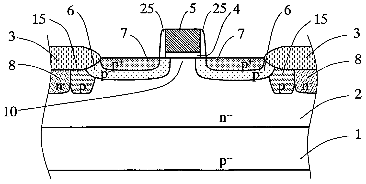
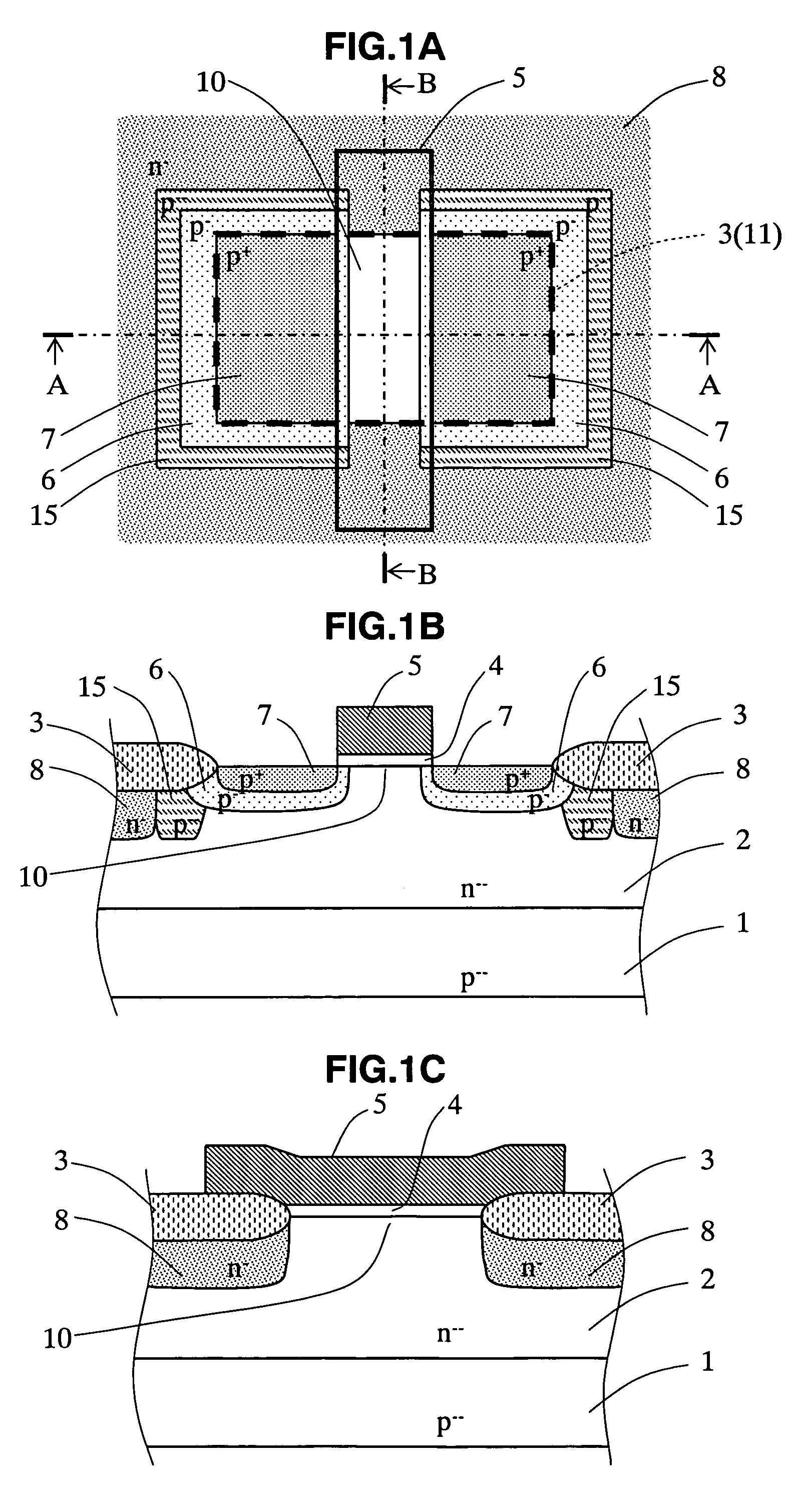
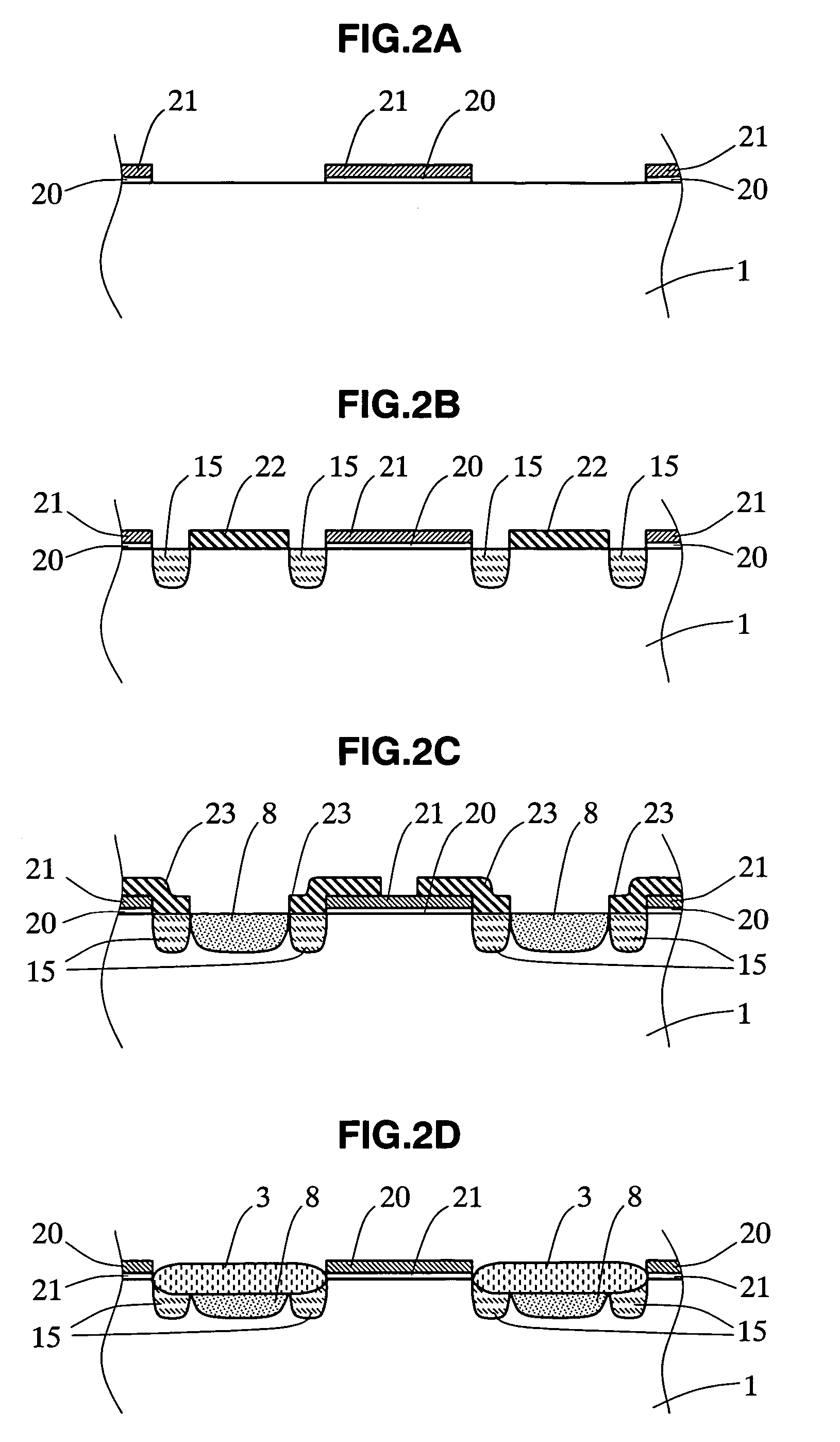
[0047]Below, a semiconductor device of an embodiment 1 of the present invention is explained in detail referring to drawings. FIG. 1A is a plane layout diagram of the semiconductor device of this embodiment, and FIGS. 1B and 1C are cross-sectional views at the A-A line and the B-B line shown in FIG. 1A, respectively. Also, FIGS. 2A to 2D and FIGS. 3A to 3D are process cross-sectional views showing the manufacturing processes of the semiconductor device shown in FIGS. 1A to 1C. In this instance, the process cross-sectional views shown in FIGS. 2A to 2D and FIGS. 3A to 3D correspond to the cross-sections at the A-A line shown in FIG. 1A. Further, FIGS. 4A to 4D are plane views corresponding to FIGS. 2A to 2D, and FIGS. 5A to 5D are plane views corresponding to FIGS. 3A to 3D. Note that in FIGS. 1A to 1C, 2A to 2D, 3A to 3D, 4A to 4D, and 5A to 5C, unlike the conventional semiconductor device explained in FIGS. 11A to 11C, a p-channel MOS transistor is shown as an example. In addition,...

embodiment 2

[0083]Next, a semiconductor device of an embodiment 2 of the present invention is explained in detail hereafter, with reference to the drawings. FIG. 10A is a plane layout diagram of the semiconductor device of this embodiment, and FIGS. 10B and C are cross-sectional views at the C-C line and the B-B line in FIG. 10A. The A-A cross-section in FIG. 10A is the same as the cross-sectional view shown in FIG. 1B. Also, FIGS. 10A to 10C illustrate a p-channel MOS transistor in the same way as in FIGS. 1A to 1C.

[0084]As shown in FIGS. 10A and 10C, the semiconductor device of this embodiment is different from the first embodiment in that in the region immediately below the gate electrode 5, the channel region 10 between the source region and the drain region projects along the gate electrode 5 toward the channel stopper region 8 (the channel stopper region 8 is retreated) and the channel region 10 is formed contacting the channel stopper region 8, and that the non-formation region 11 (a reg...


PUM


Abstract

In this invention, the semiconductor device is provided with a gate electrode formed on a gate insulating film in a region sectioned by an element isolation formed on a semiconductor layer of the first conduction type, and a source region and a drain region of the second conduction type. At least one of the source region and the drain region has a first low concentration region and a high concentration region. Also, the semiconductor device of the present invention is provided with a second low concentration region of the second conduction type between a channel stopper region formed below the element isolation and the source region, and between the channel stopper region and the drain region. The semiconductor layer immediately below the gate electrode projects to the channel stopper region side along the gate electrode, and the semiconductor layer and the channel stopper region make contact with each other.

Description

BACKGROUND OF THE INVENTION[0001]1. Field of the Invention[0002]This invention relates to a semiconductor device and a manufacturing method thereof, and more specifically, a semiconductor device suitable for mixed mounting high-voltage MOS (Metal Oxide Semiconductor) transistors and low-voltage MOS transistors, and a manufacturing method thereof.[0003]2. Description of the Related Art[0004]In forming a plurality of MOS transistors on the same semiconductor substrate, an element isolation region made of an oxide film or the like is provided between neighboring transistors to insulate them from each other. Also, below the element isolation region is provided a channel stopper region comprising an impurity region of the same conduction type as a well region.[0005]In terms of construction, if the channel stopper region is formed contacting a high-concentration impurity region comprising a source region or a drain region of an MOS transistor, when the transistor is in the operating state...

Claims


Application Information

Patent Timeline
Patent Type & Authority Patents(United States)
IPC IPC(8): H01L29/72
CPCH01L29/1083H01L29/7833B66C1/04
Inventor FUKUMOTO, AKIRAWATANABE, RIE
Owner PANNOVA SEMIC
Why Eureka
Try Eureka