Manufacture method for semiconductor device having field oxide film

A device manufacturing method and semiconductor technology, applied in the direction of semiconductor/solid-state device manufacturing, electrical components, circuits, etc., can solve problems such as inability to obtain operational effects

Inactive Publication Date: 2006-08-16
YAMAHA CORP
View PDF1 Cites 2 Cited by
  • Summary
  • Abstract
  • Description
  • Claims
  • Application Information

AI Technical Summary

Problems solved by technology

[0021] According to the above reference Figures 9A to 9C Although the field oxide film formation method of the present invention is simple in process, since the channel stop region 5B is formed to extend in the device opening 6A, the above-mentioned operational effects (a) and (b) cannot be obtained.

Method used


Image

  • Manufacture method for semiconductor device having field oxide film
  • Manufacture method for semiconductor device having field oxide film
  • Manufacture method for semiconductor device having field oxide film

Examples


Embodiment Construction

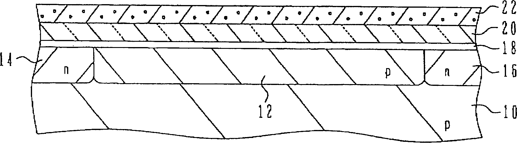
[0066] Figures 1A to 1J A method of manufacturing a metal oxide semiconductor (MOS) type integrated circuit (IC) using the field oxide film forming method according to the first embodiment of the present invention is shown. will be described in turn corresponding to Figures 1A to 1J craft.

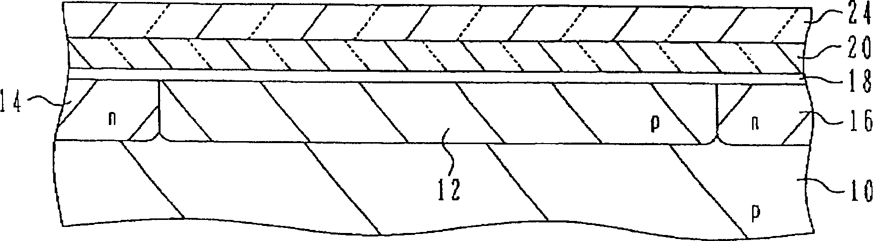
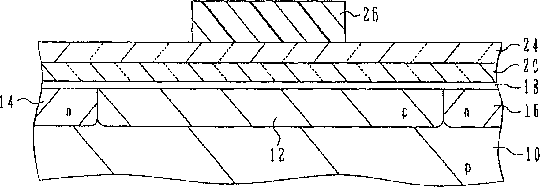
[0067] exist Figure 1A In the process shown, p-type well region 12 and n-type well regions 14 and 16 are formed side by side on the main surface of p-type silicon substrate 10 by a known method. The n-type well regions 14 and 16 may be formed as one well region surrounding the p-type well region 12 . After well regions 12 to 16 are formed, silicon oxide film (stress relaxation pad oxide film) 18 is formed on the main surface of substrate 10 by thermal oxidation. The thickness of silicon oxide film 18 may be, for example, in the range from 30 nm to 40 nm. A silicon nitride film 20 is formed on the silicon oxide film 18 by CVD, and a polysilicon film 22 is formed on the silicon nitri...


PUM

PropertyMeasurementUnit
thicknessaaaaaaaaaa
thicknessaaaaaaaaaa
thicknessaaaaaaaaaa

Abstract

To provide a method of forming a field oxide film capable of simply and accurately forming a channel stopper region separately from an element hole immediately under the field oxide film. On the principal surface of a silicon substrate, a side spacer made of silicon nitride is formed on the side wall of a lamination including a silicon oxide film, a silicon nitride film and a silicon oxide film. Thereafter, a channel stopper ion doped region is formed by implanting impurity ions by using as a mask the lamination, side spacer and resist layer. After the resist layer and side spacer are removed, a field oxide film is formed through selective oxidation using the lamination as a mask, and a channel stopper region corresponding to the ion doped region is formed. After the lamination is removed, a circuit device such as a MOS type transistor is formed in each device opening of the field oxide film.

Description

technical field [0001] The present invention relates to a method for forming a field oxide film (insulating film) suitable for the manufacture of a metal oxide semiconductor (MOS) type integrated circuit (IC), and more particularly relates to a method for forming a field oxide film located only in a field oxide film. technology of the channel stop region below and separated from the device opening. Background technique [0002] known use Figures 7A to 7C The shown method of the lateral spacer is a conventional method of forming a field oxide film having a channel stopper region located only under the field oxide film and separated from the device opening (see, for example, JP-A-HEI-5-136123 ). [0003] exist Figure 7A In the shown process, after the surface of the p-type silicon substrate 1 is thermally oxidized to form a silicon oxide film 2, a silicon nitride film 3 is formed on the silicon oxide film 2 by chemical vapor deposition (CVD), and the silicon nitride film 3...

Claims


Application Information

Patent Timeline
Patent Type & Authority Applications(China)
IPC IPC(8): H01L21/76
Inventor 高见秀诚深见博昭
Owner YAMAHA CORP
Why Eureka
Try Eureka