Copper on organic solderability preservative (OSP) interconnect

a preservative and organic soldering technology, applied in the direction of semiconductor devices, semiconductor/solid-state device details, electrical apparatus, etc., can solve the problems of low bonding reliability and device performance, high heat generation, and high electrical resistan

Inactive Publication Date: 2009-01-08
UNITED TEST & ASSEMBLY CENT LTD
View PDF10 Cites 50 Cited by
  • Summary
  • Abstract
  • Description
  • Claims
  • Application Information

AI Technical Summary

Problems solved by technology

During bonding, the Au and Al inter-diffuse into each other and may result in high electrical resistance and high heat generation.
This may then lead to low bonding reliability and device performance.
Also, the poor heat dissipation characteristic of gold materials may cause overheating in the IC assembly.
Furthermore, Au materials have low tensile strength and may result in poor wire sagging, poor wire sweeping performance, poor wire loop profile and instability for long wires, during packing encapsulation.
Another problem that may occur in wire bonding is that the bond pad surface on the chip or the lead finger surface on the substrate may have oxidized material coated thereon, which may decrease bonding reliability.

Method used


Image

  • Copper on organic solderability preservative (OSP) interconnect
  • Copper on organic solderability preservative (OSP) interconnect
  • Copper on organic solderability preservative (OSP) interconnect

Examples


Embodiment Construction

[0053]Hereinafter, exemplary embodiments of the present invention will be described with reference to the accompanying drawings.

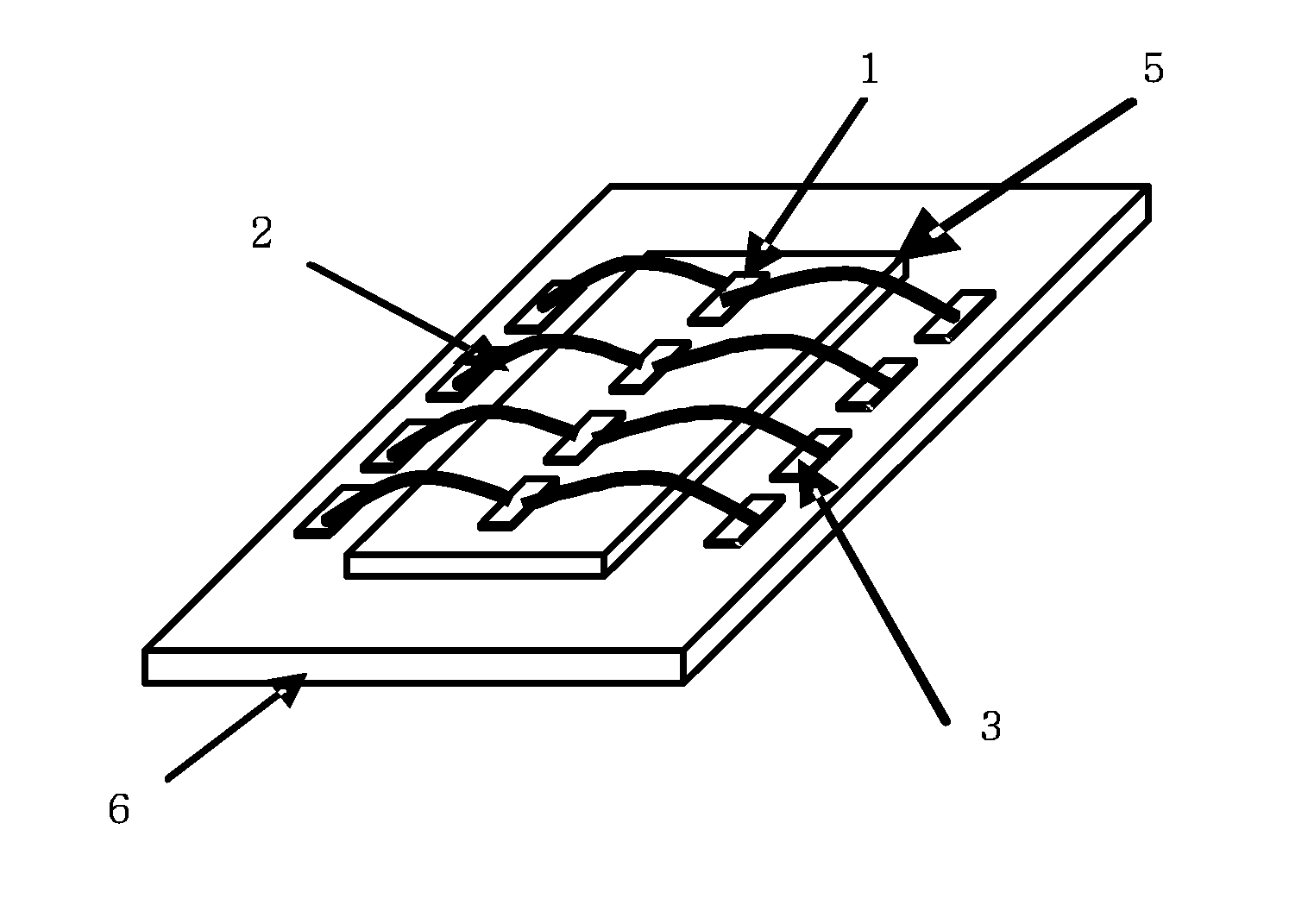
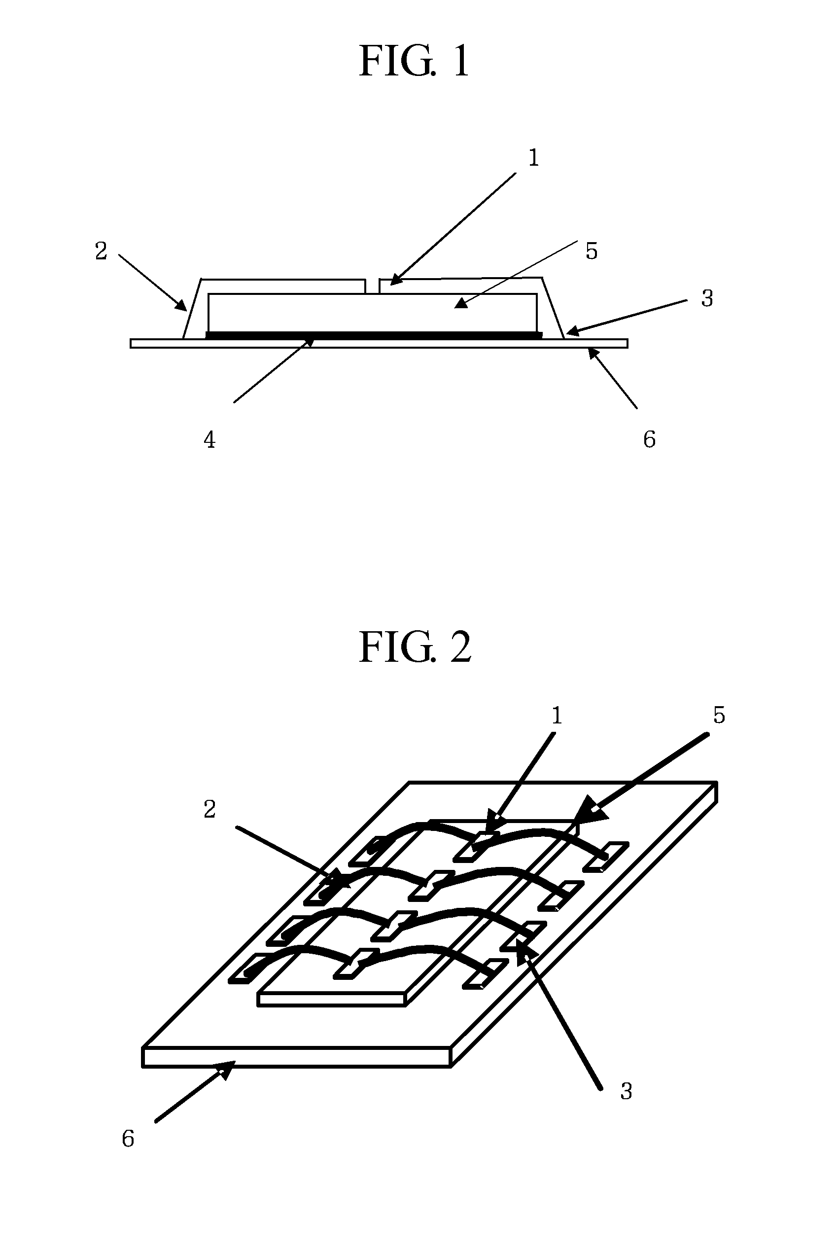
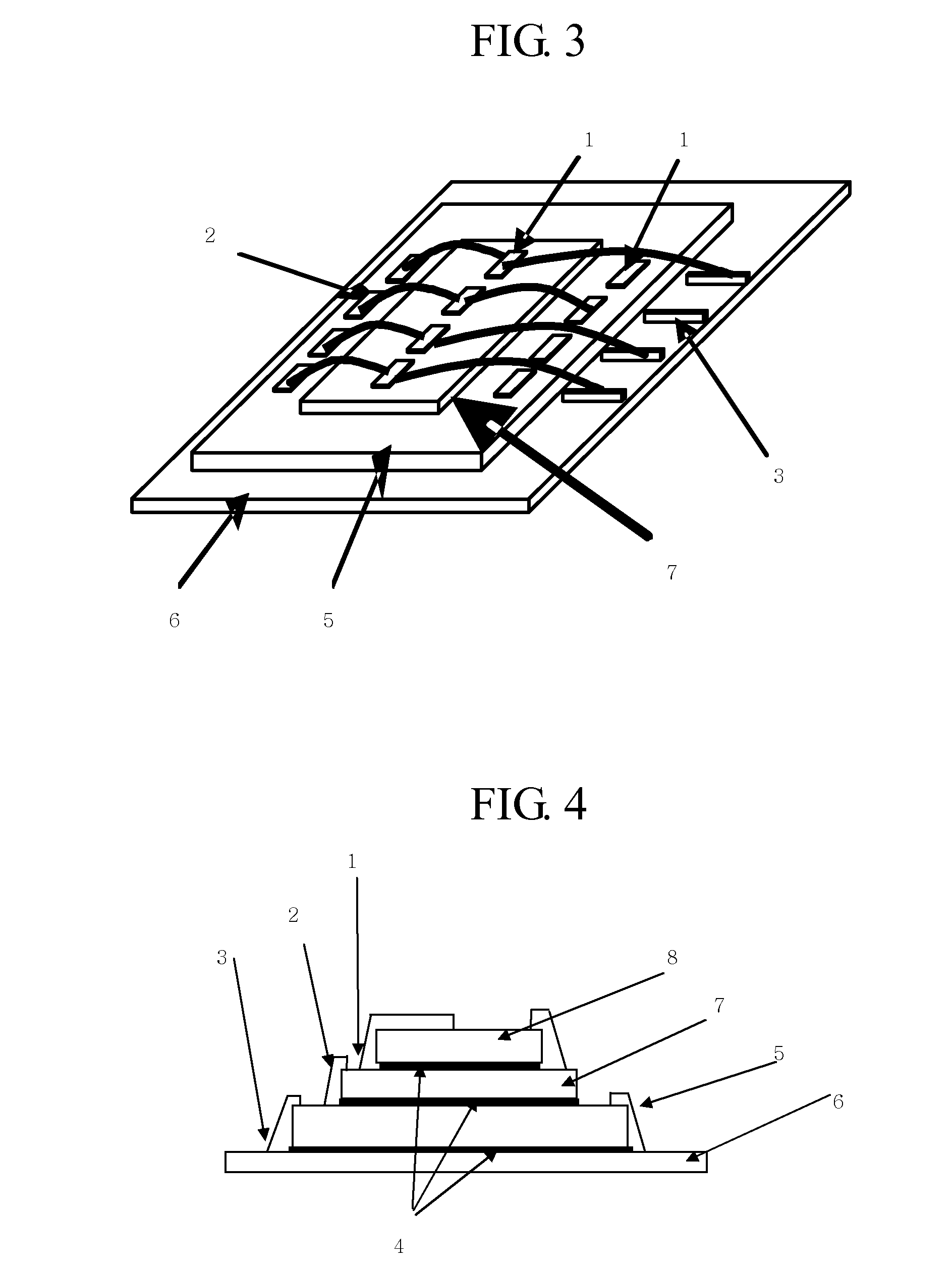
[0054]FIG. 1 illustrates a semiconductor package according to an exemplary embodiment of the present invention.

[0055]As shown in FIG. 1 the semiconductor package according to an exemplary embodiment of the present invention includes bond pads 1, copper wires 2, lead fingers 3, adhesive material 4, a semiconductor chip 5, and an OSP substrate 6.

[0056]The adhesive material 4 is used to provide adhesion between the semiconductor chip 5 and the OSP substrate 6.

[0057]The OSP substrate 6 is coated in an OSP material, and the copper wire 2 is wire bonded through the OSP material to a lead finger 3 of the OSP substrate 6. The substrate may be a lead frame material (e.g., Alloy 42, Cu7025, Olin 0194, and other copper alloys), PCB, substrate core material (e.g., BT832, Hitachi E679, Nanya NPG-150), glass panel or ceramic material. The OSP coating on the substrate 6 m...


PUM

PropertyMeasurementUnit
electricalaaaaaaaaaa
electrical resistanceaaaaaaaaaa
heat dissipationaaaaaaaaaa

Abstract

Provided is a semiconductor package, and a method for constructing the same, including a first substrate, a first semiconductor chip attached to the first substrate, and a first copper wire. At least one of the first substrate and the first semiconductor chip has an Organic Solderability Preservative (OSP) material coated on at least a portion of one surface, and the first copper wire is wire bonded through the OSP material to the first substrate and the first semiconductor chip.

Description

CROSS-REFERENCE TO RELATED APPLICATIONS[0001]This application claims priority from U.S. Provisional Application No. 60 / 882,710 filed on Dec. 29, 2006 and U.S. Provisional Application No. 60 / 951,018 filed on Jul. 20, 2007, the disclosures of which are incorporated herein by reference.BACKGROUND OF INVENTION[0002]1. Field of Invention[0003]Apparatuses and methods consistent with the present invention relate to Copper (Cu) wire bonding through Organic Solderability Preservative (OSP) material that coats a substrate and / or through OSP material that coats a chip bond pad.[0004]2. Description of the Related Art[0005]Wire bonding is generally a means of electrical connection between a semiconductor chip and a substrate. The substrate may, for example, be a printed circuit board (PCB) or a lead frame. Wire bonding typically involves using gold (Au) wire, aluminum (Al) wire, Cu wire, silver (Ag) wire, or a combination of alloy wire to form the electrical connection.[0006]Au wire is commonly ...

Claims


Application Information

Patent Timeline
Patent Type & Authority Applications(United States)
IPC IPC(8): H01L23/49H01L21/44
CPCH01L24/05H01L24/06H01L24/45H01L24/48H01L24/49H01L25/0657H01L2224/04042H01L2224/05073H01L2224/05553H01L2224/05624H01L2224/05639H01L2224/05647H01L2224/06136H01L2224/32145H01L2224/45014H01L2224/45124H01L2224/45139H01L2224/45144H01L2224/45147H01L2224/48091H01L2224/48095H01L2224/48145H01L2224/48227H01L2224/4824H01L2224/48463H01L2224/4847H01L2224/48475H01L2224/48505H01L2224/48624H01L2224/48639H01L2224/48647H01L2224/48824H01L2224/48839H01L2224/48847H01L2224/49H01L2224/73215H01L2224/73265H01L2224/85051H01L2224/85375H01L2225/0651H01L2225/06582H01L2924/01005H01L2924/01013H01L2924/01028H01L2924/01029H01L2924/01047H01L2924/01079H01L2924/01082H01L2924/01327H01L2924/014H01L2924/09701H01L2924/14H01L2924/19043H01L2924/19107H01L2924/01033H01L2924/01068H01L2224/48724H01L2224/48739H01L2224/48747H01L2224/48479H01L2224/06135H01L2924/00014H01L2924/00H01L2224/48471H01L24/85H01L2924/00011H01L2924/10161H01L2924/00015H01L2924/01049H01L2224/4554H01L2924/00012H01L2924/206H01L2224/43848H01L2224/45015H01L2924/207
Inventor ENG, KIAN TENGJOHANNES HETZEL, WOLFGANGJOSEF REISS, WERNERAMMER, FLORIANCHUAN KOH, YONGSIAT, JIMMY
Owner UNITED TEST & ASSEMBLY CENT LTD
Why Eureka
Try Eureka