

Reflowed solder ball with low melting point metal cap
- Summary
- Abstract
- Description
- Claims
- Application Information
AI Technical Summary
Benefits of technology
Problems solved by technology
Method used
Image

Examples
example 1
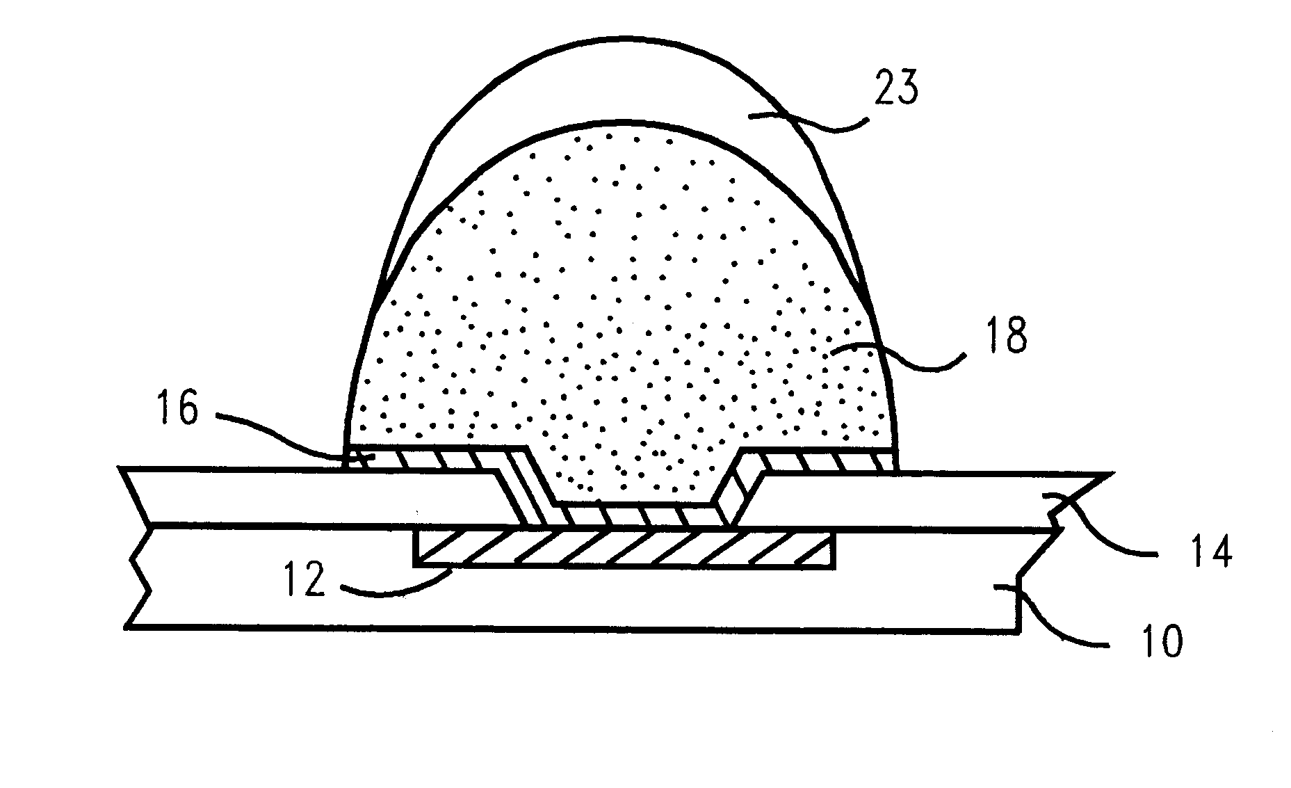
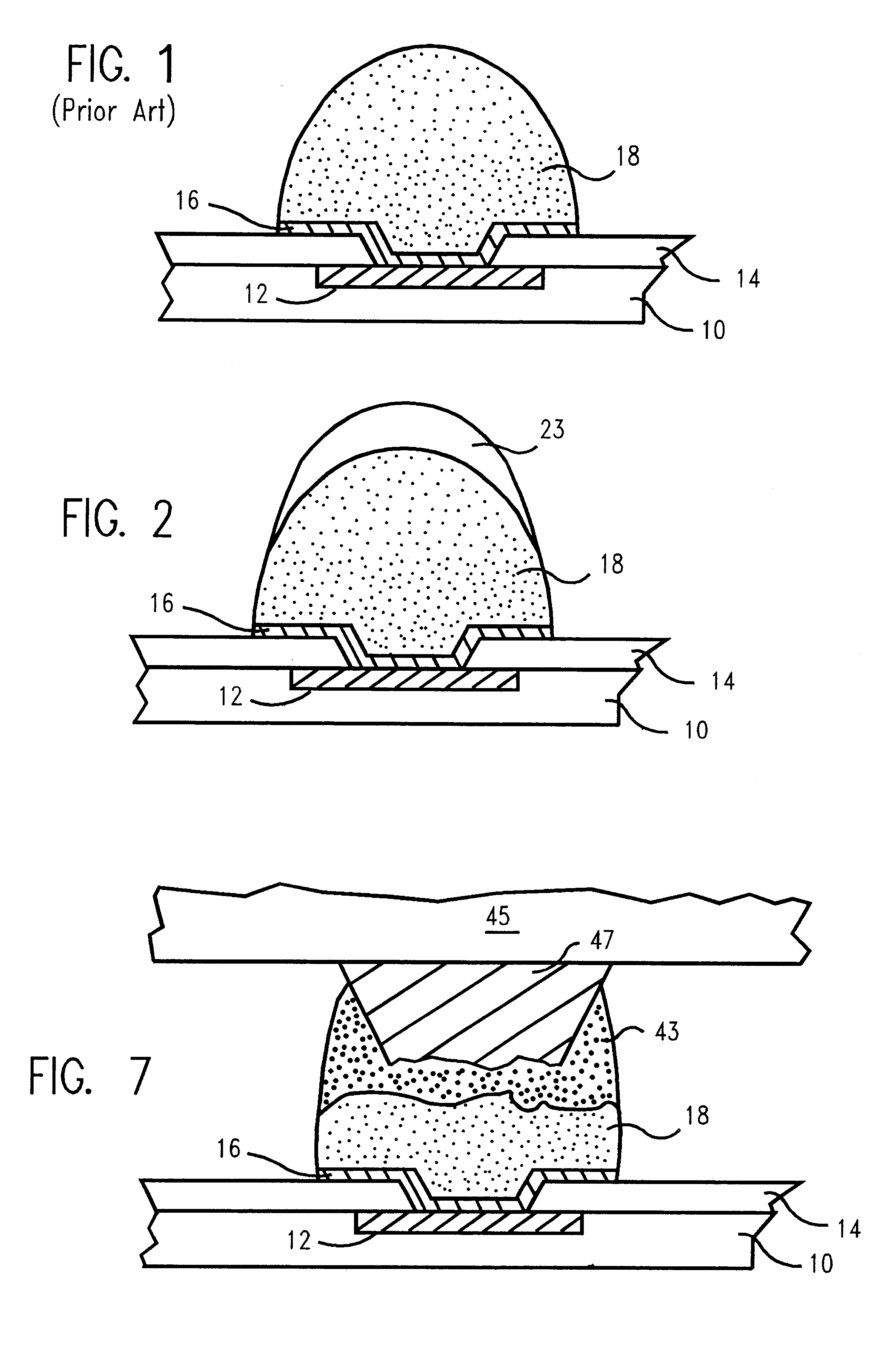
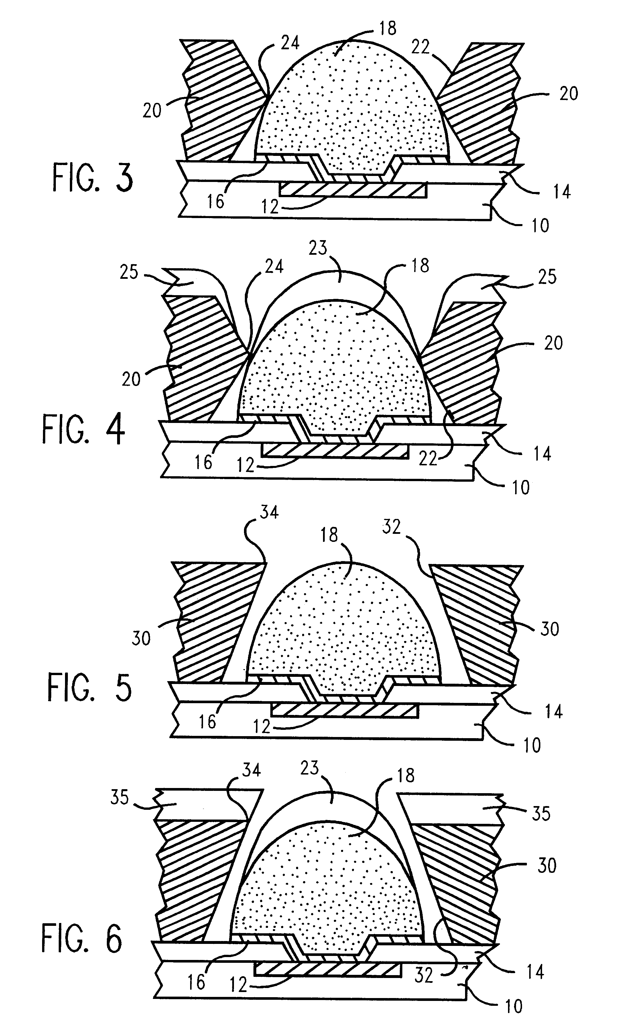
Semiconductor modules were made using the structure and process of this invention. On a conventional solder ball 18, a capping layer of tin 23, was formed. The deposited capping layer of pure tin was between about 0.5 to about 2.0 mil thick, and it was deposited by evaporation. The amount of tin to be deposited on the solder ball 18, was determined by the volume of eutectic solder that is required to completely cover the exposed copper conductors 47, in card or substrate 45. The width and thickness of the copper conductor and the solder mask opening determines the surface area and hence the required eutectic volume. A 20 to 35 cubic mil of eutectic solder 43, volume is preferred for an original 40 to 100 cubic mil of high melt solder ball 18, volume.
PUM
 Abstract
Description
Claims
Application Information