Charging device
- Summary
- Abstract
- Description
- Claims
- Application Information
AI Technical Summary
Benefits of technology
Problems solved by technology
Method used
Image

Examples
Embodiment Construction
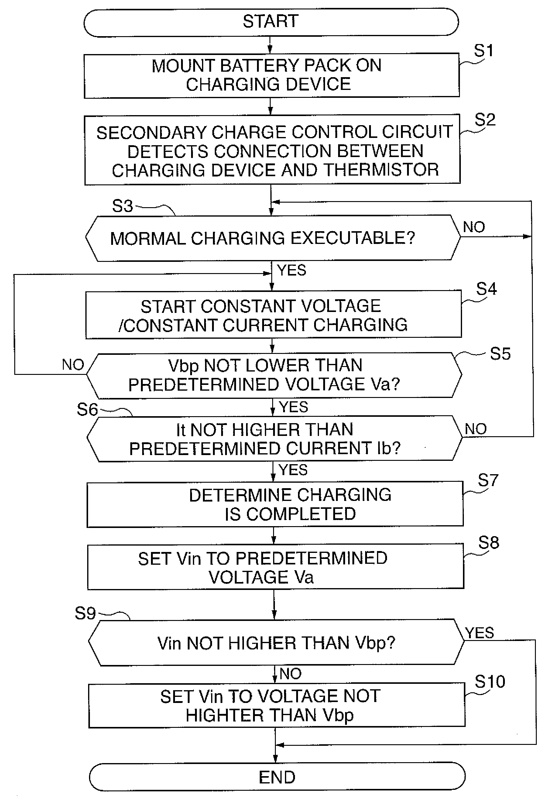
[0018]The present invention will now be described in detail below with reference to the accompanying drawings showing embodiments thereof.
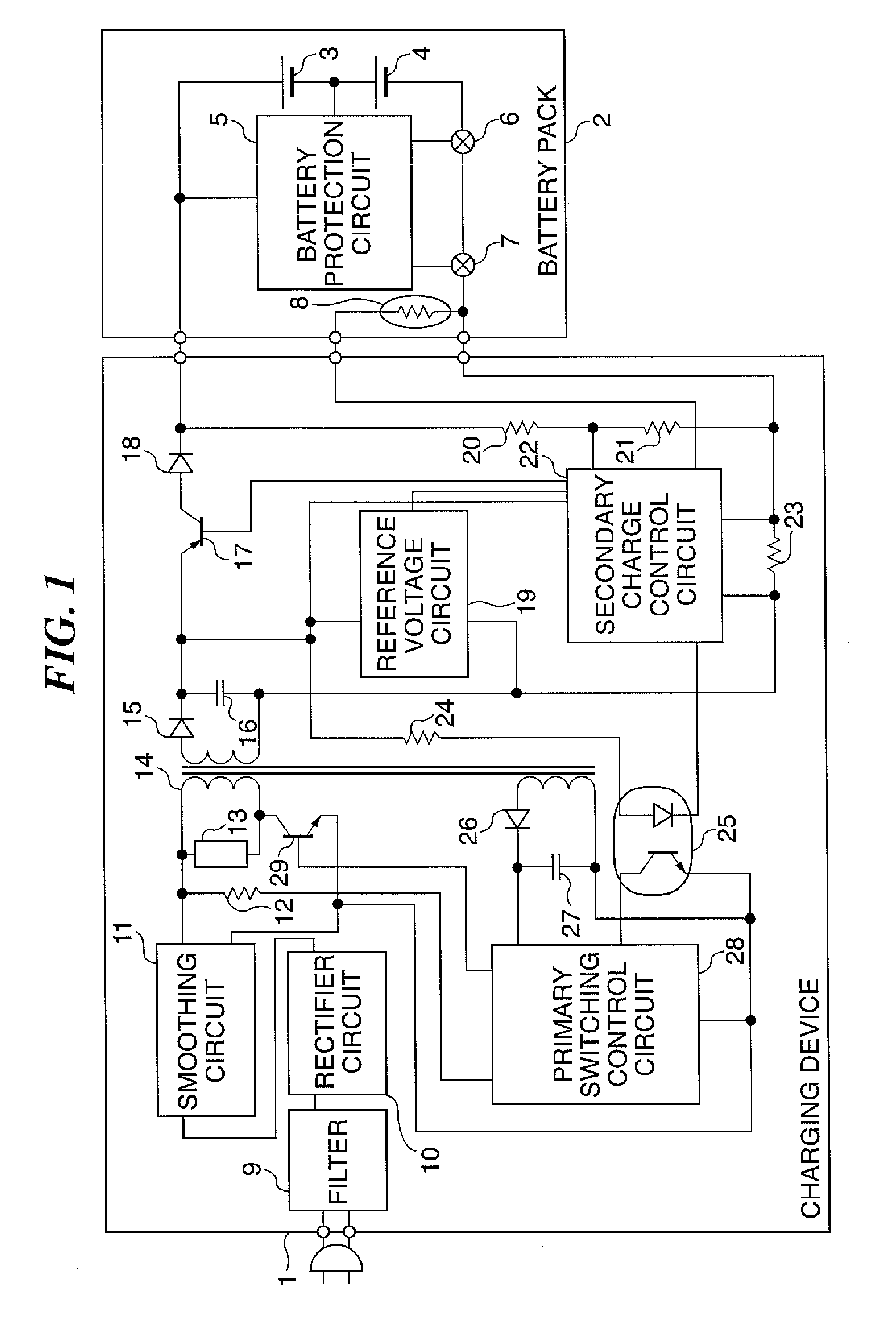
[0019]FIG. 1 is a schematic diagram of the circuit configuration of a charging device according to a first embodiment of the present invention and a battery pack that can be mounted on the charging device.
[0020]First, a description will be given of the battery pack.
[0021]The battery pack 2 is configured to be attachable to and detachable from the charging device 1 that performs constant voltage / constant current charging, and is comprised of lithium ion secondary battery cells 3 and 4, a battery protection circuit 5, semiconductor switches 6 and 7, and a thermistor 8.
[0022]The lithium ion secondary battery cells 3 and 4 are lithium ion secondary batteries which have the same characteristics and the same capacity, and are connected in series to each other. The battery protection circuit 5 performs on / off control of the semiconductor switches 6 and 7...
PUM
 Abstract
Description
Claims
Application Information
 - Generate Ideas
- Intellectual Property
- Life Sciences
- Materials
- Tech Scout
- Unparalleled Data Quality
- Higher Quality Content
- 60% Fewer Hallucinations
Browse by: Latest US Patents, China's latest patents, Technical Efficacy Thesaurus, Application Domain, Technology Topic, Popular Technical Reports.
© 2025 PatSnap. All rights reserved.Legal|Privacy policy|Modern Slavery Act Transparency Statement|Sitemap|About US| Contact US: help@patsnap.com