

Thin film transistor and manufacturing method of the same
- Summary
- Abstract
- Description
- Claims
- Application Information
AI Technical Summary
Benefits of technology
Problems solved by technology
Method used
Image

Examples
Embodiment Construction
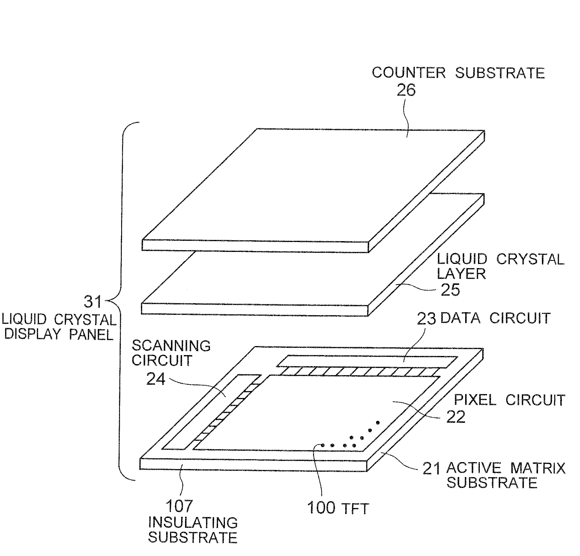
[0027]FIG. 1 is a sectional view showing a first exemplary embodiment of a TFT according to the invention. Explanations will be provided hereinafter by referring to the drawing.
[0028]A TFT 100 according to this exemplary embodiment basically includes: a light-shielding film 113 formed on a glass substrate that serves as an insulating substrate 107; an insulating film 112 formed on the light-shielding film 113; a semiconductor film 111 formed on the insulating film 112; and a gate insulating film 104 formed on the semiconductor film 111. Each layer of a laminate 100a that is configured with three layers of the light-shielding film 113, the insulating film 112, and the semiconductor film 111 is patterned simultaneously. Further, each layer of the laminate 100a is configured with silicon or a material containing silicon. The light-shielding film 113 is made of a-Si, and the film thickness thereof is 10 nm, for example. The insulating film 112 is made of SiO2, and the film thickness the...
PUM
 Abstract
Description
Claims
Application Information