Unlock instant, AI-driven research and patent intelligence for your innovation.

Clock data recovery and synchronization in interconnected devices

a clock data and clock data technology, applied in the field of computation-efficient clock data recovery and synchronization in systems with interconnected devices, can solve the problems of reducing affecting the integrity of data, and reducing the complexity of input/output pins, so as to reduce the overhead of communication and reduce the complexity. , the effect of not sacrificing the accuracy of synchronization

Inactive Publication Date: 2009-01-15
YIN JOHN +1
View PDF14 Cites 53 Cited by
  • Summary
  • Abstract
  • Description
  • Claims
  • Application Information

AI Technical Summary

Benefits of technology

[0014]An advantage of the present invention is the reduced complexity in a system of interconnected devices and lower communications overhead. Another advantage is that the accuracy of the synchronization is not sacrificed in order to achieve lower complexity. Another advantage is that the lower complexity reduces system cost.
is the reduced complexity in a system of interconnected devices and lower communications overhead. Another advantage is that the accuracy of the synchronization is not sacrificed in order to achieve lower complexity. Another advantage is that the lower complexity reduces system cost.

Problems solved by technology

The major drawback of parallel connections among multiple processing devices is a proliferation of input / output (I / O) pins.
A loss of synchronization may jeopardize the integrity of the data.
This is a disadvantage for some applications.
For example, in a digital radio system, transferring the received analog signal from an antenna or analog front end (AFE) to the ADC requires expensive cables for radio frequency (RF) signals.
However, the digital signal processing portion would require a computationally expensive CDR module for the digital link.
Each CDR module includes a computationally expensive PLL.
In addition, not all FPGA PLLs have the same capability.
Other FPGA devices have PLLs with lesser functionality that do not support CDR operations.
For systems with multiple interconnected devices, the cost and complexity for communication among devices increases for every channel.
This produces scalability problems, where the overhead for communication becomes prohibitive.
Therefore, the PLL is the most expensive resource on the FPGA.

Method used


Image

  • Clock data recovery and synchronization in interconnected devices
  • Clock data recovery and synchronization in interconnected devices
  • Clock data recovery and synchronization in interconnected devices

Examples


Embodiment Construction

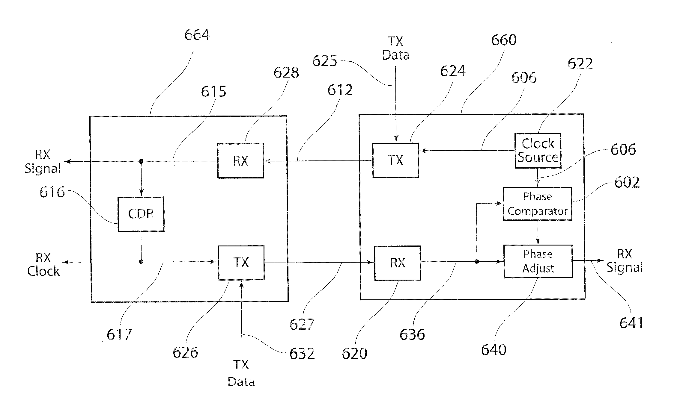
[0033]In any interconnected system, data transfer between devices requires the receiving device to synchronize to signals received from the transmitting device. FIG. 1 shows an example of an interconnected system that includes a master device 104 with serial links 101 and 102 to a slave device 100. The master device 104 and the slave device 100 each include a CDR module, 108 and 106, respectively, to recover the clock from the their respective received signals. As described above in the Background section, the PLL required for conventional CDR can consume a prohibitive amount of resources. Current solutions for this situation include commercially available matched chip sets. FIG. 2 shows a block diagram of a matched chip set where each chip, 206 and 208, provides an interface between the respective devices 200 and 204 and the respective links, 202 and 210. The matched chips 206 and 208 perform the CDR functions, including the PLL, and provide the recovered clocks 212 and 214 and the...


PUM


Abstract

For synchronizing a master device and a slave device connected by a data transfer link, the master device measures a phase offset in a signal received from the slave device with respect to the master's clock signal. The master determines a control symbol based on the phase offset. The master encodes the control symbol in a transmit signal for the slave. The slave decodes the control symbol from the signal received from the master. The slave uses the control symbol to adjust the phase shift to compensate for the phase offset of a signal to be transmitted to the master device. When the phase compensated signal is received at the master, its phase offset is smaller than the original phase offset. This procedure can be performed iteratively until the phase offset is within a desired tolerance.

Description

BACKGROUND OF THE INVENTION[0001]This invention relates to computationally efficient clock data recovery and synchronization in systems with interconnected devices having high rates of data transfer between devices.[0002]Several trends in system design are increasing the demand for data transfer in interconnected devices. The volume of data requiring transfer between digital devices are constantly increasing, driving a requirement for higher data transfer rates. As an example, more digital signal processing applications are being performed by field programmable gate arrays (FPGAs) instead of conventional digital signal processors. System designs require more interconnections between FPGA devices and between FPGA devices and other devices. In the past, interface architectures among multiple devices have typically used parallel connections. The major drawback of parallel connections among multiple processing devices is a proliferation of input / output (I / O) pins. To avoid this, the tre...

Claims


Application Information

Patent Timeline
IPC IPC(8): H03L7/00
CPCH03L7/06H04L7/02H04J3/0685
Inventor YIN, JOHNHOYER, BRYAN H.
Owner YIN JOHN
Features
  • R&D
  • Intellectual Property
  • Life Sciences
  • Materials
  • Tech Scout
  • Unparalleled Data Quality
  • Higher Quality Content
  • 60% Fewer Hallucinations
Learn More