Integrated circuit with multiple layers of circuits

a technology of integrated circuits and layers, applied in the field of integrated circuits, can solve the problems of increased post-manufacture (field) failure of integrated circuits, excessive yield loss, and difficulty in over-stressing integrated circuits, and achieve the effect of reducing the overhead level

Active Publication Date: 2009-01-15
ARM LTD
View PDF0 Cites 17 Cited by
  • Summary
  • Abstract
  • Description
  • Claims
  • Application Information

AI Technical Summary

Benefits of technology

[0007]The present technique recognises that by using a three dimensional integration technique whereby a plurality of layers of circuits with a corresponding layout are superimposed this permits redundant circuits to be located directly above or below the circuits for which they are providing redundancy. The circuit blocks within a stack will normally be substantially identical or at least provide the same signal interface and functionality so as to be able to substitute for one another. This physical location within a stack of circuits allows for a relatively easy retrofit into existing architectures and designs and provides an advantageously low signal routing overhead associated with the use of the redundant circuit blocks when needed.
[0020]Whilst the above soft error protection technique could be provided for every state holding element, such as every memory cell within a memory, it may also be used more selectively to provide a good deal of soft error protection with a significantly reduced level of overhead by protecting only strategic state holding elements, such as the register file within a microprocessor, the input and output buffers from a memory system or integrated circuit.

Problems solved by technology

Furthermore, there is an increased problem of post-manufacture (field) failures of integrated circuits due to wear out caused by electromigration and oxide breakdown (among other factors).
These failures are made worse by the difficulties related to manufacture-time burn-in; it is increasingly difficult to over-stress integrated circuits at manufacture-time to find integrated circuits that are likely to fail early in the field as such techniques incur too many false positives causing excessive yield loss.
A further factor is the increasing uncertainty associated with manufactured structures: it is becoming increasingly difficult to be confident that measurement / test conditions are sufficiently like operating conditions to give valid information such that subsequent failures are often due to variability rather than any particular break-down effect.
However, such traditional fault tolerance techniques require significant modification of the integrated circuit architecture of many designs representing a significant and disadvantageous cost.
Furthermore, the use of such fault tolerance techniques (such as triple modular redundancy) tends to be expensive in the terms of the associated circuit overhead.

Method used


Image

  • Integrated circuit with multiple layers of circuits
  • Integrated circuit with multiple layers of circuits
  • Integrated circuit with multiple layers of circuits

Examples


Embodiment Construction

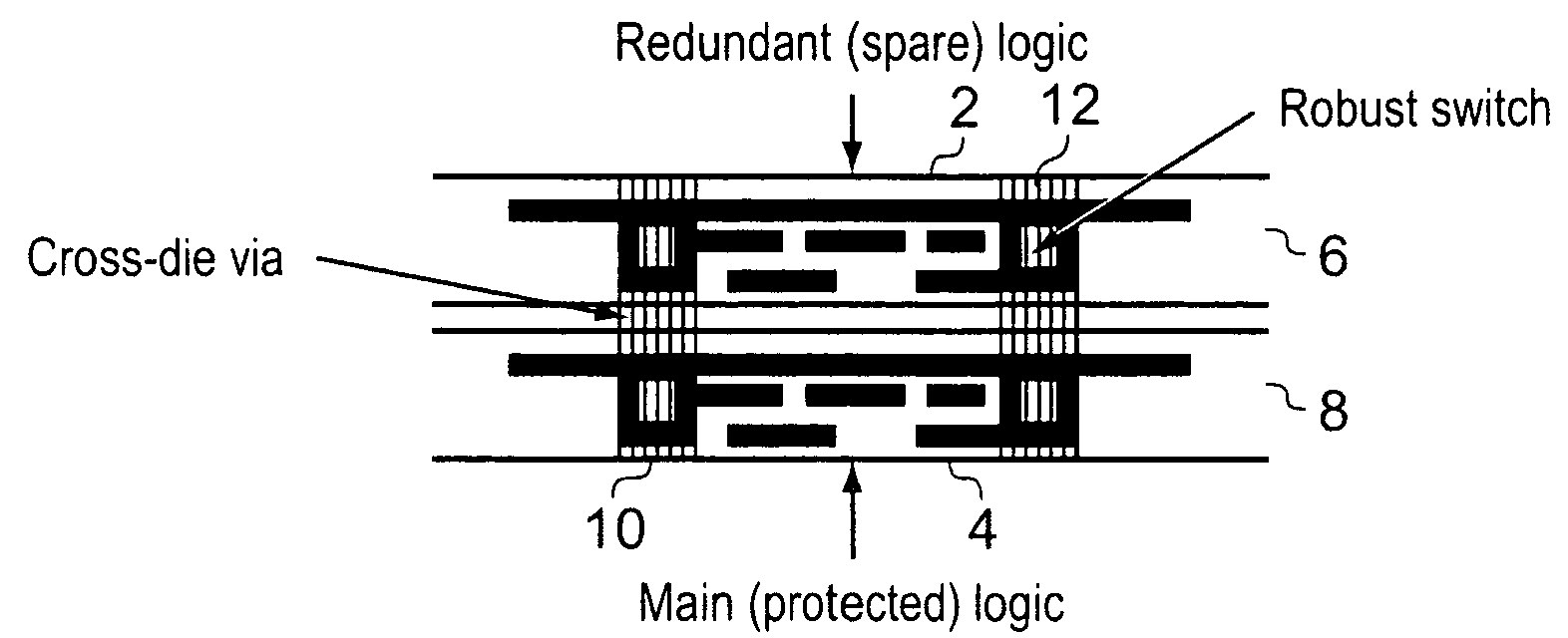
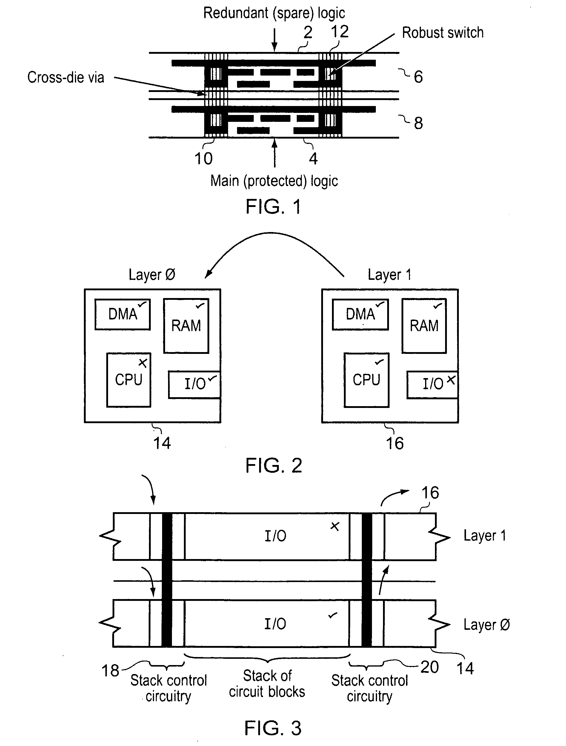
[0042]FIG. 1 schematically illustrates two circuit blocks 2, 4 which have a substantially identical form and functionality. It will be appreciated that the two circuit blocks 2, 4 may vary slightly due to manufacturing variations or may vary more markedly such as through the use of different manufacturing parameters, such as being manufactured to have different threshold switching voltages or with different doping characteristics, but physically with the same size components. The physical correspondence between the two circuit blocks 2, 4, and the corresponding layouts of the layers of circuits 6, 8 within which they are formed, enable the layers of circuits 6, 8 to be superimposed such that the circuit blocks 2, 4 are adjacent one another and form a stack. A cross-die via 10 is used to link together points at which input signals pass into the circuit blocks 2, 4 and a further cross-die via 12 can be used to link together points at which output signals leave the circuit blocks 2, 4....


PUM

PropertyMeasurementUnit
Electrical resistanceaaaaaaaaaa
Sizeaaaaaaaaaa
Speedaaaaaaaaaa

Abstract

An integrated circuit 78 is formed of multiple layers of circuits 14, 16 superimposed to produce stacks of circuit blocks 2, 4. Stack control circuitry 18, 20 is associated with the input and output signals from the circuit blocks to direct these to / from the currently active circuit block(s) as appropriate. The superimposed circuit blocks 2, 4 provide redundancy for each other, both for manufacturing defect resistance and for operational redundancy, such as providing multiple modular redundancy in safety critical environments.

Description

BACKGROUND OF THE INVENTION[0001]1. Field of the Invention[0002]This invention relates to the field of integrated circuits. More particularly, this invention relates to integrated circuits formed of multiple layers of circuits.[0003]2. Description of the Prior Art[0004]As the process size with which integrated circuits are manufactured has become smaller fault tolerance is becoming increasingly important factor in integrated circuit design. Furthermore, there is an increased problem of post-manufacture (field) failures of integrated circuits due to wear out caused by electromigration and oxide breakdown (among other factors). These failures are made worse by the difficulties related to manufacture-time burn-in; it is increasingly difficult to over-stress integrated circuits at manufacture-time to find integrated circuits that are likely to fail early in the field as such techniques incur too many false positives causing excessive yield loss. A further factor is the increasing uncert...

Claims


Application Information

Patent Timeline
IPC IPC(8): H01L25/00H01S4/00
CPCH01L25/0657H01L2225/06513H01L2225/06527Y10T29/49002H01L2924/0002H01L2225/06541H01L2924/00
Inventor FLAUTNER, KRISZTIANAITKEN, ROBERT CAMPBELLHILL, STEPHEN JOHN
Owner ARM LTD
Why Eureka
Try Eureka