Semiconductor apparatus and manufacturing method thereof

a technology of semiconductor apparatus and manufacturing method, which is applied in the direction of electrical apparatus, semiconductor device details, semiconductor/solid-state device devices, etc., can solve the problems of complicated manufacturing step of semiconductor apparatus, and achieve the effects of improving reliability of the finally obtained semiconductor apparatus, good wettability between metal wires and conductive pastes, and improving reliability of the semiconductor apparatus

Inactive Publication Date: 2009-01-22
SHINKO ELECTRIC IND CO LTD
View PDF11 Cites 40 Cited by
  • Summary
  • Abstract
  • Description
  • Claims
  • Application Information

AI Technical Summary

Benefits of technology

[0029]Also, in the semiconductor apparatus according to the invention, the side surface wiring is formed by applying the conductive paste containing conductive particles, so that its side surface wiring can easily be formed as compared with a related-art semiconductor apparatus in which the side surface wiring is formed using a vapor deposition method and a liftoff method.
[0030]In the case of making contact between the metal wire and the conductive paste thus, wettability between the metal wire and the conductive paste is good, so that the conductive paste tends to be gathered on a peripheral surface of the corresponding metal wire and can be prevented from being in contact with the adjacent side surface wiring. Thus, reliability of the finally obtained semiconductor apparatus can be improved.
[0031]Moreover, a part of the conductive paste applied to the side surfaces of the plural stacked semiconductor elements can easily enter a gap between the adjacent semiconductor elements and is formed on the tapered surface, and thus, makes contact with a metal wire extended along the tapered surface. As a result of that, the metal wire whose one end is connected to the electrode terminal of the semiconductor element can surely make contact with the side surface wiring and reliability of the semiconductor apparatus can be more improved.

Problems solved by technology

Therefore, in the related-art semiconductor apparatus in which plural semiconductor elements are stacked, a normal semiconductor element in which an electrode terminal is formed on its one surface cannot be used and a manufacturing step of the semiconductor apparatus is complicated.

Method used


Image

  • Semiconductor apparatus and manufacturing method thereof
  • Semiconductor apparatus and manufacturing method thereof
  • Semiconductor apparatus and manufacturing method thereof

Examples


Embodiment Construction

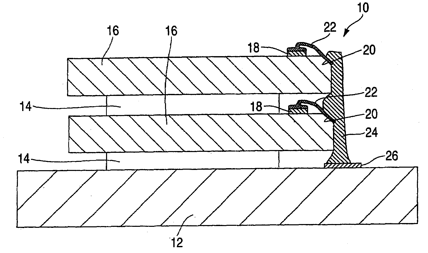
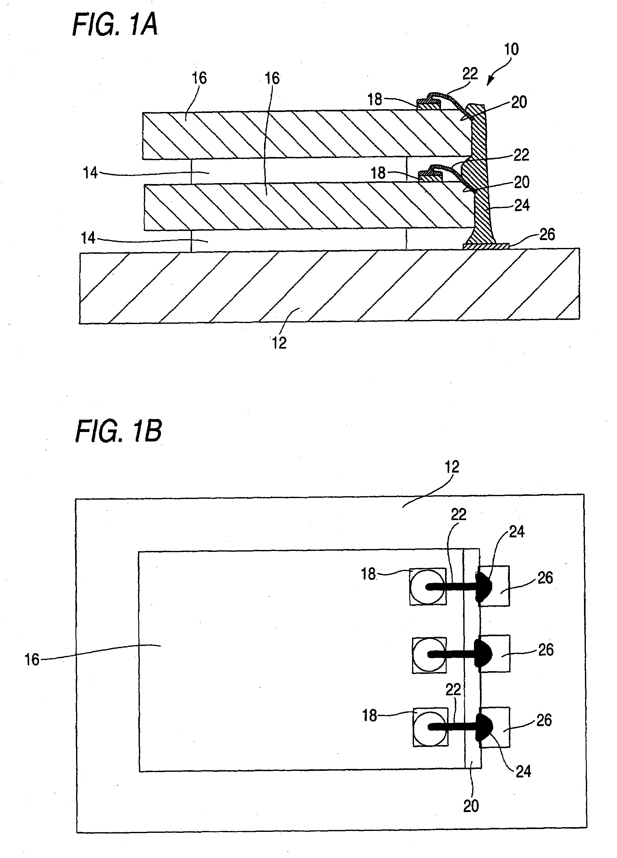
[0045]FIGS. 1A and 1B show one example of a semiconductor apparatus according to the invention. FIG. 1A is a schematic sectional view of a semiconductor apparatus 10, and FIG. 1B is a schematic plan view of the semiconductor apparatus 10. In the semiconductor apparatus 10 shown in FIG. 1, semiconductor elements 16, 16 are stacked on one surface of a circuit substrate 12 through adhesive layers 14, 14.

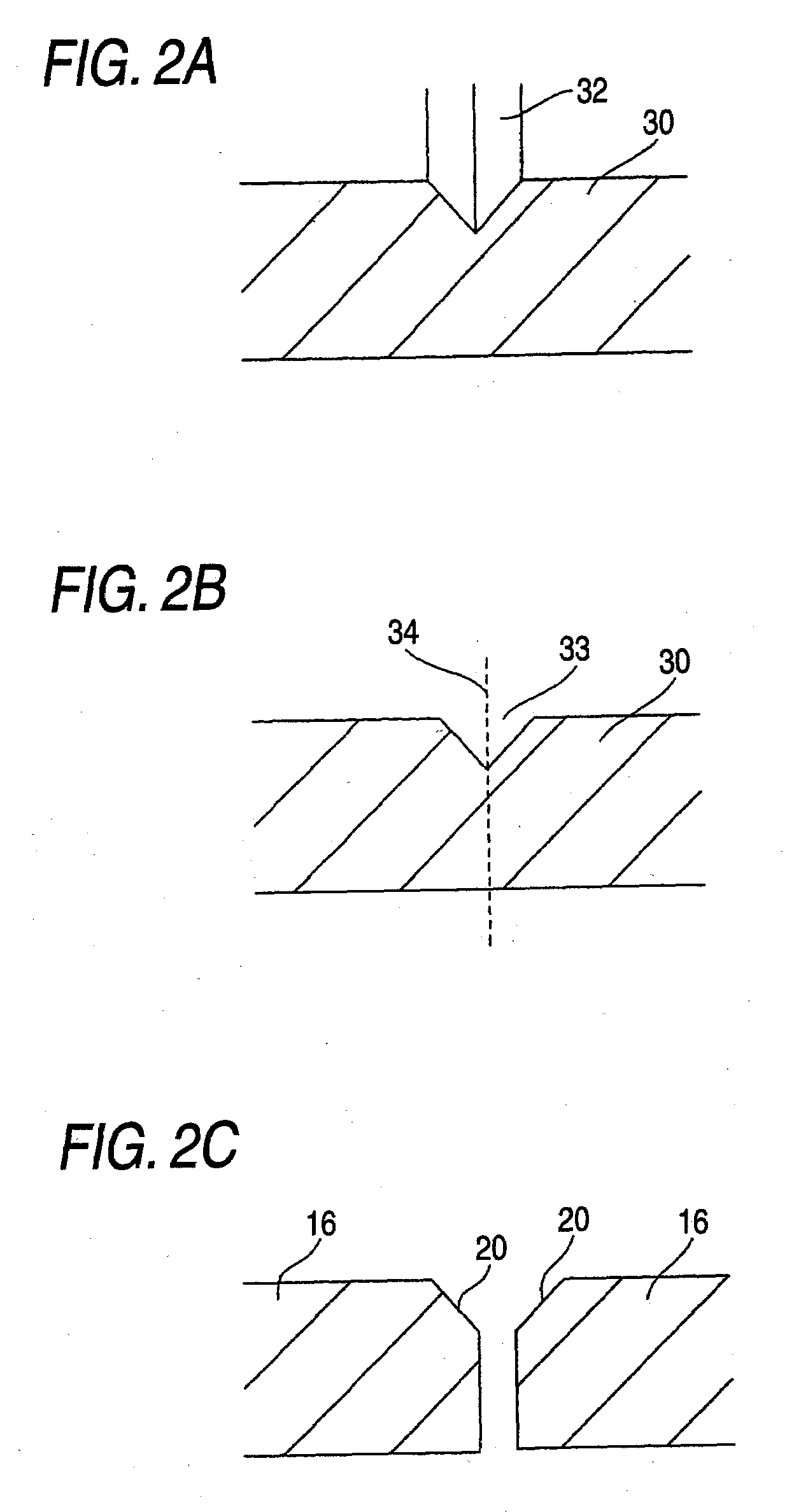
[0046]Each of such semiconductor elements 16, 16 is a quadrilateral-shaped semiconductor element in which electrode terminals 18, 18, . . . are formed on one surface of the semiconductor element (which is referred as electrode terminal formation surface). A tapered surface 20 is formed by cutting off an edge of the electrode terminal formation surface, on which the electrode terminals 18, 18, . . . are formed, among edges formed along each of sides of this semiconductor element 16. In this embodiment, the tapered surface 20 is formed by cutting off the edge which is closer to the electr...


PUM


Abstract

A plurality of quadrilateral-shaped semiconductor elements are stacked on the one surface of a circuit substrate. A side surface wiring for making electrical connection between each of the electrode terminals of the semiconductor elements and a pad formed on the circuit substrate is formed by applying a conductive paste containing conductive particles. A metal wire whose one end is connected to the electrode terminal is extended along a tapered surface formed by cutting off an edge of the electrode terminal surface on which the electrode terminal is formed among edges formed along each of the sides of the semiconductor element. At least a part of the metal wire extended from each of the electrode terminals of the semiconductor elements to the tapered surface is electrically connected to the side surface wiring.

Description

TECHNICAL FIELD[0001]The present disclosure relates to a semiconductor apparatus and a manufacturing method thereof. More particularly, the present disclosure relates to a semiconductor apparatus in which plural quadrilateral-shaped semiconductor elements are stacked on one surface of a circuit substrate and also a side surface wiring for making electrical connection between each of electrodes of the semiconductor elements and a pad formed on the circuit substrate is formed, and a manufacturing method thereof.RELATED ART[0002]Density growth has been achieved by arranging semiconductor elements 100, 100 in three dimensions as described in a semiconductor apparatus shown in FIG. 11 with capacity and density growth of a recent semiconductor apparatus. In the semiconductor apparatus shown in FIG. 11, the semiconductor elements 100, 100 are stacked on one surface of a wiring substrate 102 through adhesive layers 104, 104. Wire bonding between pads of the wiring substrate 102 and electrod...

Claims


Application Information

Patent Timeline
Patent Type & Authority Applications(United States)
IPC IPC(8): H01L23/52H01L21/00
CPCH01L21/6835H01L2224/76152H01L24/45H01L24/48H01L24/78H01L24/82H01L24/85H01L24/91H01L25/0657H01L29/0657H01L2224/24145H01L2224/45144H01L2224/48091H01L2224/4813H01L2224/48227H01L2224/48465H01L2224/48471H01L2224/48599H01L2224/73265H01L2224/78301H01L2224/85001H01L2224/85181H01L2225/06551H01L2225/06575H01L2924/01004H01L2924/01005H01L2924/01006H01L2924/01007H01L2924/01013H01L2924/01029H01L2924/01047H01L2924/01079H01L2924/01082H01L2924/10157H01L2924/30105H01L24/24H01L2924/01033H01L2924/01023H01L2924/00014H01L2924/00H01L2224/05554H01L2224/4554H01L2224/85399H01L2224/05599H01L23/12
Inventor MURAYAMA, KEIMIZUNO, SHIGERUKURIHARA, TAKASHISHIRAISHI, AKINORIHIGASHI, MISUTOSHI
Owner SHINKO ELECTRIC IND CO LTD
Why Eureka
Try Eureka