Light emitting device and method of manufacturing the same

a technology of light emitting devices and manufacturing methods, applied in the direction of discharge tubes/lamp details, discharge tubes luminescnet screens, electric discharge lamps, etc., can solve the problems of color unevenness, difficult to form multi-layered structures including phosphor layers and transparent resin layers on a flat substra

Inactive Publication Date: 2009-01-22
KK TOSHIBA
View PDF6 Cites 72 Cited by
  • Summary
  • Abstract
  • Description
  • Claims
  • Application Information

AI Technical Summary

Problems solved by technology

However, in such a white LED light emitting device, since phosphor particles are evenly distributed, light emission color becomes more yellowish as an optical path from the LED chip through a phosphor layer becomes longer, which may result in undesired color unevenness.
However, in this structure, since the phosphor layer contacts the LED chip, there arises a problem in that the LED chip absorbs light emitted from the phosphor layer and the phosphor layer absorbs heat generated by the LED chip.
However, the above-mentioned multi-layered structure including the phosphor layer and the transparent resin layer requires a complicated process, and moreover, it is very difficult to form the multi-layered structure including the phosphor layer and the transparent resin layer on a flat substrate.

Method used


Image

  • Light emitting device and method of manufacturing the same
  • Light emitting device and method of manufacturing the same
  • Light emitting device and method of manufacturing the same

Examples


first embodiment

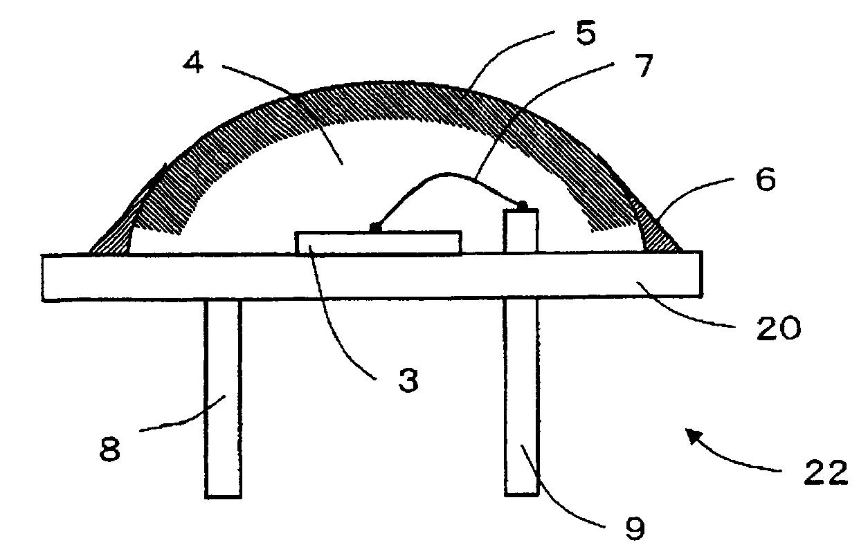
[0021]A white LED light emitting device according to a first embodiment of the invention includes a substrate 20, an LED chip 3 which is an excitation light source of a phosphor and is mounted on the substrate 20, a transparent resin layer (transparent resin portion) 4 formed on the substrate 20 in a shape of dome (for example, semispherical shape) to cover the LED chip 3, and a phosphor layer 5 formed on an outer side of the transparent resin layer 4, as shown in FIG. 1. A ring-shaped region having no phosphor layer 5 is provided in an outer side of a portion near a boundary between the semi-spherical transparent resin layer 4 and the substrate 20. A reflecting layer 6 is formed to cover this region. The LED chip 3 is connected to electrodes 8 and 9 on a lead frame 22 by means of a gold wire boding 7 or the like.

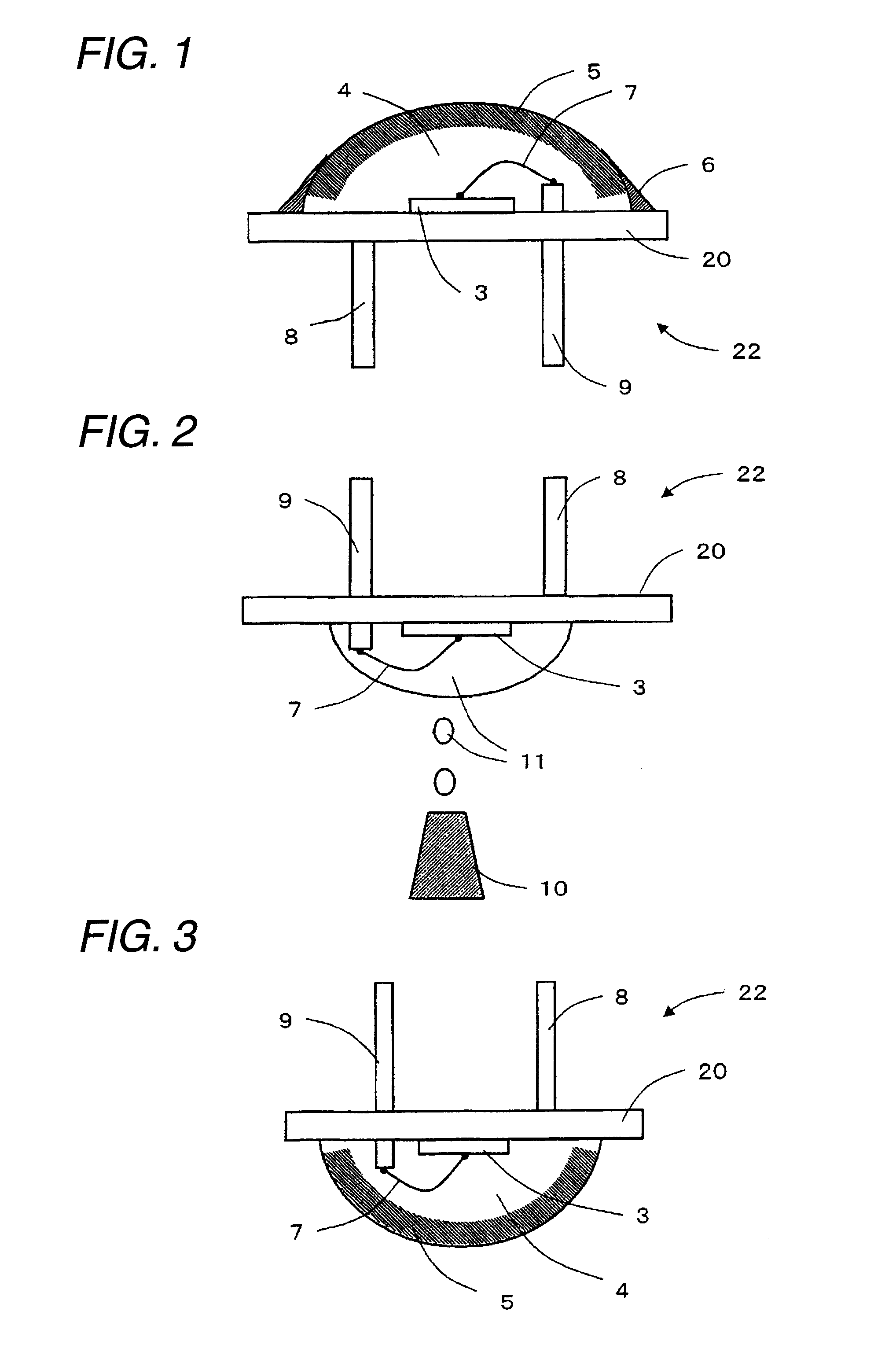
[0022]The LED light emitting device as constructed above is manufactured according to an order as shown in FIGS. 2 to 4, for example. First, the LED chip 3 is mounted on th...

second embodiment

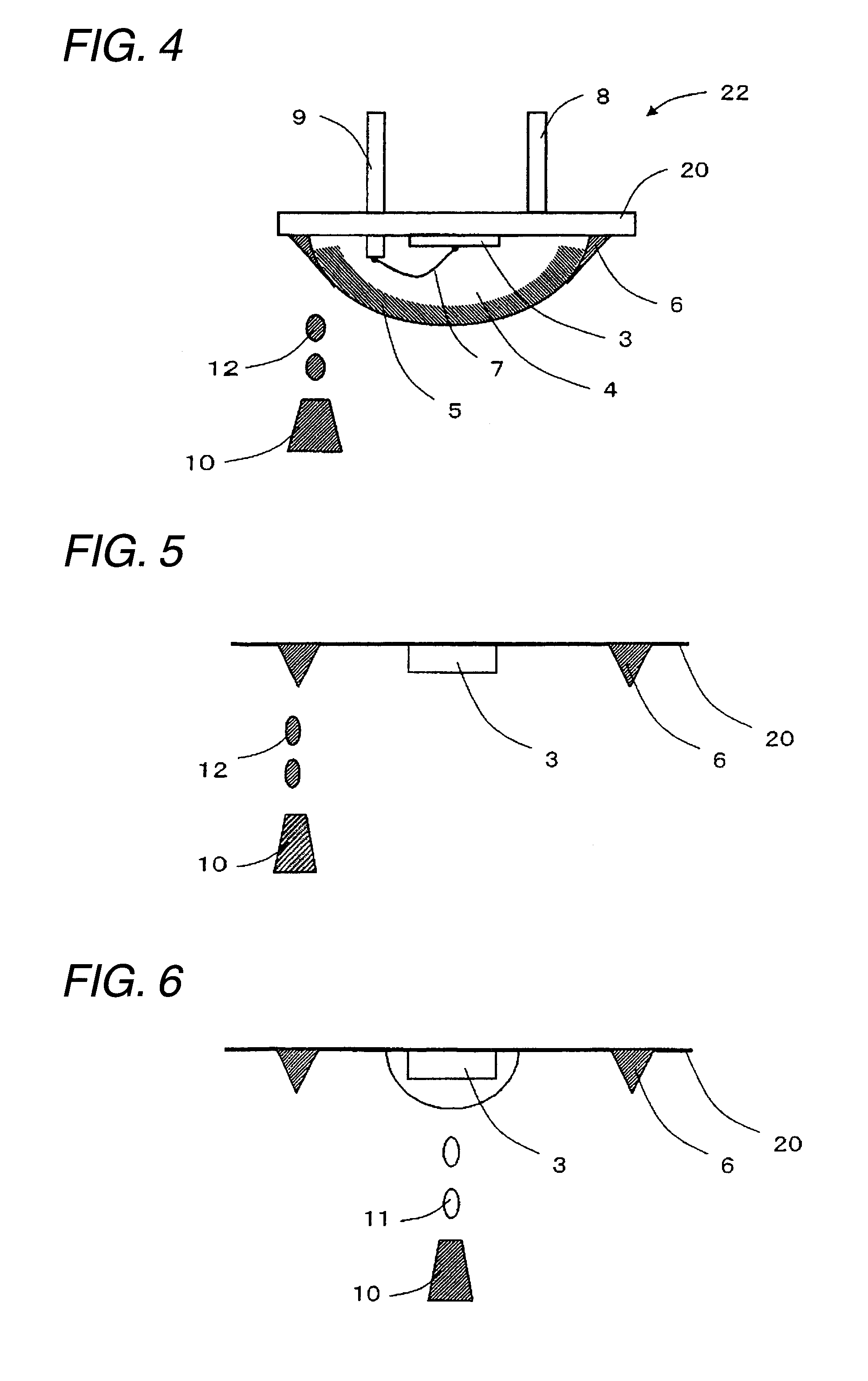
[0042]As shown in FIGS. 5 to 7, the processes of forming the white LED light emitting device structure as described above may be changed in an order. Specifically, the LED chip 3 is first mounted on the substrate, and then, as shown in FIG. 5, the reflecting layer 6 is formed by coating the metal-containing ink 12 on the flat substrate 20 in a ring shape by means of the liquid droplet discharging apparatus 10. At this tome, by discharging and coating the metal-containing ink having high viscosity on the flat substrate 20 by means of, particularly an ultrasonic type liquid droplet discharging apparatus 10, it becomes easy to a cubic structure of the reflecting layer 6 having a thickness in a direction perpendicular to the substrate 20.

[0043]Subsequently, as shown in FIG. 6, a dome is formed by discharging the phosphor-containing transparent resin 11 on the LED chip formed on the substrate 20. Thereafter, the transparent resin is cured after the phosphor is precipitated. Thus, the whi...

third embodiment

[0044]The manufacturing method of the present invention may be applied to manufacturing a light emitting device using a package cup having a reflecting plate, as shown in FIG. 8. In this embodiment, a package cup 30 having a depressed portion 31 is used instead of a flat substrate, and the LED chip 3 is mounted on the center of the bottom 32 of the depressed portion 31. Next, the semi-spherical transparent resin layer 4 and phosphor layer 5 are formed in the outer side of the LED chip 3, and the ring-shaped reflecting layer 6 is formed near a boundary between the transparent resin layer 4 and the bottom 32 of the depressed portion 31.

[0045]In this embodiment, like the first or second embodiment, the transparent resin layer 4, the phosphor layer 5 and the reflecting layer 6 are formed by discharging liquid droplets upward by means of the liquid droplet discharging apparatus 10 under a state where the depressed portion 31 of the package cup 30 on which the LED chip 3 is mounted is dir...


PUM

PropertyMeasurementUnit
diameteraaaaaaaaaa
diameteraaaaaaaaaa
viscosityaaaaaaaaaa

Abstract

A method of manufacturing a light emitting device. The method includes: mounting a light emitting chip on a substrate; forming a transparent resin portion and a phosphor layer by using a liquid droplet discharging apparatus, the transparent resin portion being formed in a shape of a dome and covering the light emitting chip to fill an exterior thereof on the substrate, a phosphor layer containing phosphor and being formed on an exterior of the transparent resin portion close to at least a top side thereof; and forming a reflecting layer at a position exterior of the transparent resin portion and the phosphor layer close to the substrate.

Description

[0001]The entire disclosure of Japanese Patent Application No. 2007-132552 filed on May 18, 2007 including specification, claims, drawings and abstract is incorporated herein by reference in its entirety.BACKGROUND OF THE INVENTION[0002]1. Field of the Invention[0003]The present invention relates to a light emitting device including a light emitting diode (LED) chip mounted on a substrate, and a phosphor-containing transparent resin arranged in an exterior of the LED chip, and a method of manufacturing the light emitting device.[0004]2. Description of the Related Art[0005]There has been known a white LED light emitting device produced by a combination of an LED chip emitting excited light of a low wavelength and phosphor particles having wavelength conversion performance, in which the LED chip is mounted on a substrate attached with a reflecting plate and a transparent resin layer in which yellow phosphor particles are dispersed is coated on the LED chip (see JP-A-7-99345). However,...

Claims


Application Information

Patent Timeline
Patent Type & Authority Applications(United States)
IPC IPC(8): H01L21/00H01J1/62H01L33/56H01L33/50H01L33/60H01L33/62
CPCH01L33/46H01L33/507H01L33/54H01L2933/0041H01L2224/45144H01L2224/48091H01L2924/00014H01L2924/00
Inventor TAKASU, ISAONOMURA, YUKOHIOKI, TSUYOSHIAMEMIYA, ISAOABE, KAZUHIDE
Owner KK TOSHIBA
Why Eureka
Try Eureka