Assembly substrate and method of manufacturing the same

a technology of assembly substrate and assembly method, which is applied in the direction of final product manufacturing, sustainable manufacturing/processing, and semiconductor/solid-state device details. it can solve the problems of poor substrate strength, affecting the quality of assembly, and inevitably occurring warpage of worksheets, so as to improve enhance the strength of substrate, and suppress the effect of warpag

Active Publication Date: 2009-01-29
TDK CORPARATION
View PDF6 Cites 6 Cited by
  • Summary
  • Abstract
  • Description
  • Claims
  • Application Information

AI Technical Summary

Benefits of technology

[0023]According to the assembly substrate of the present invention and its manufacturing method, since the substrate strength is enhanced substantially isotropically without extreme local difference (that is, without directional anisotropy), uneven internal stress is relaxed and the substrate strength is improved further, enabling warpage of the substrate to be suppressed, and handling at the time of manufacturing / processing such as transferring and separating to be facilitated. Moreover, when the assembly substrate is separated on a line so as to cross each of the concave portions in the frame body, substrate pieces (worksheets, or individual substrates) on which cut pieces of the frame body are present in a shape of a frame at its outer periphery (outer edge) can be produced at a low cost and in a simple manner without requiring a complicated steps, while reducing the load on the separating tool. Therefore, occurrence of disadvantages at the time of transferring, separating, build-up, or surface mounting can be suppressed, enabling enhancement of productivity and economic efficiency, such as improvement of yield, and improvement of mounting reliability to be achieved.

Problems solved by technology

With the conventional worksheet manufacturing method described above, warpage of a worksheet inevitably occurs due to stress applied during the formation of the insulation layers.
When the above-mentioned conventional manufacturing method is applied to the production of such work boards, since a frame-like conductive pattern is provided discontinuously, resultant work boards may have poor substrate strength in a portion not provided with frame-like conductive patterns, resulting in handling difficulty at the time of manufacturing / processing including transferring and separating as well as insufficient suppression of warpage.
It is expected that these problems will be significant further as the work board becomes thinner and has a larger area.
On the other hand, with the frame-like conductive pattern removed, each of the worksheets obtained by separating the work board will have significantly lower substrate strength in comparison to the work board, resulting in handling difficulty and warpage which is not suppressed at all.
As a result, inconveniences such as transfer failures and degraded positional accuracy at the time of build-up and surface mounting may occur.
Therefore, when the above-mentioned conventional manufacturing method is applied to the production of a work board, not only reduction of productivity and economic efficiency, such as a decline in process yield, but also a decline in the mounting reliability will occur.

Method used


Image

  • Assembly substrate and method of manufacturing the same
  • Assembly substrate and method of manufacturing the same
  • Assembly substrate and method of manufacturing the same

Examples


first embodiment

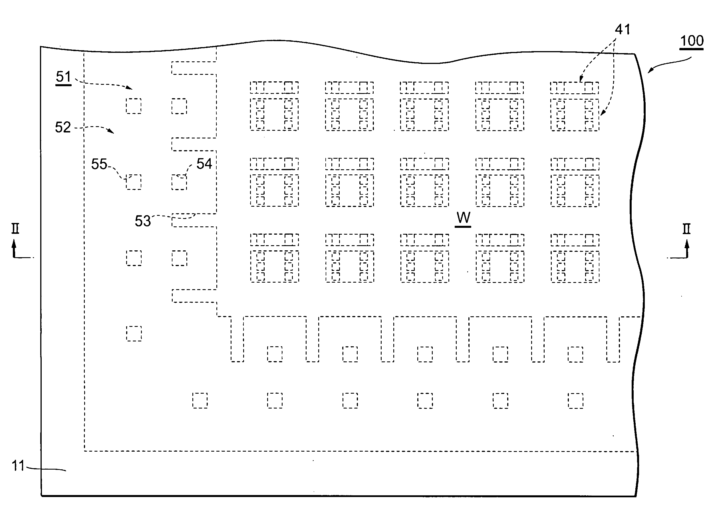
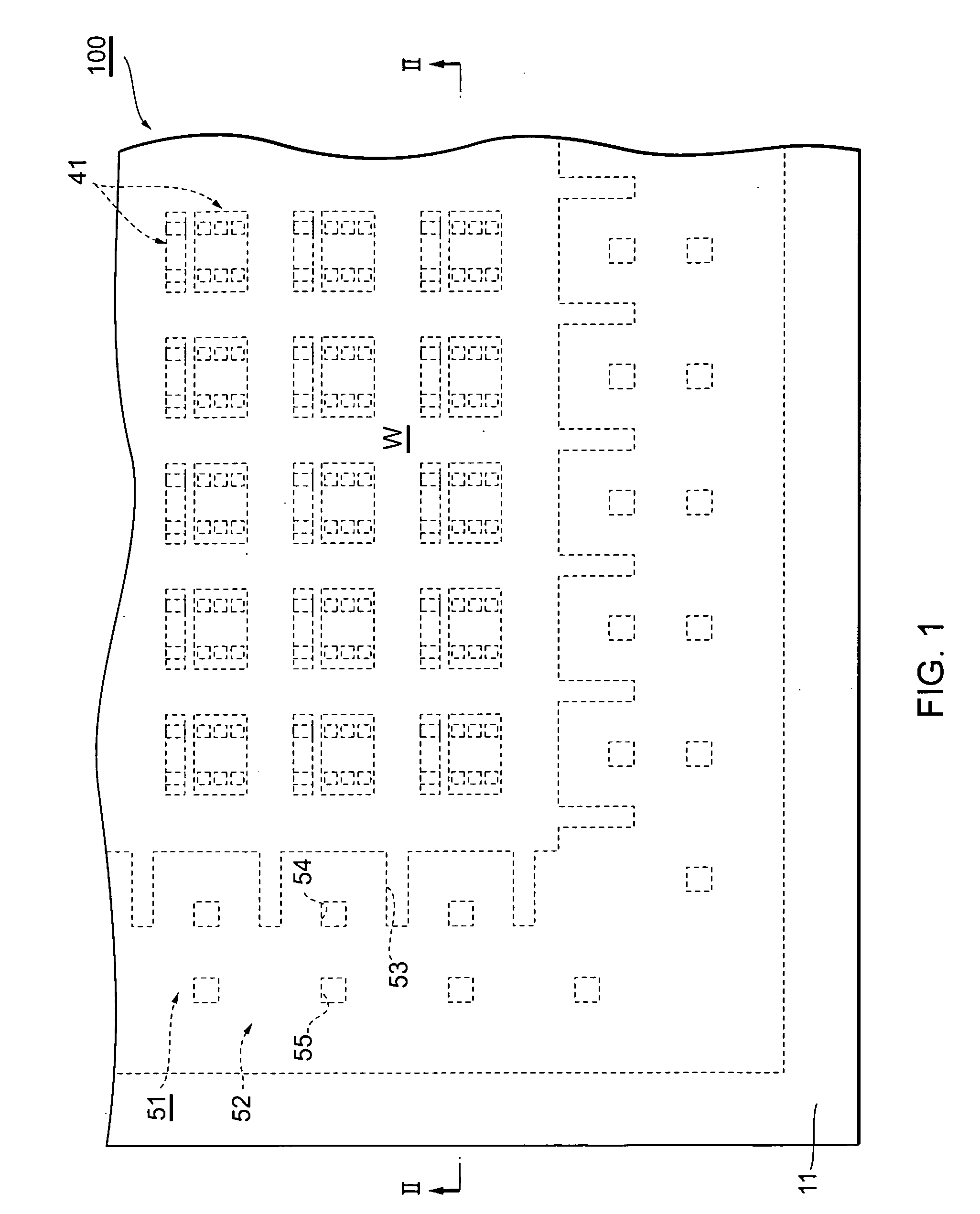
[0054]FIG. 1 and FIG. 2 are a main part enlarged plan view and a main part enlarged cross-sectional view schematically illustrating the structure of a first embodiment of the assembly substrate according to the present invention, respectively. A work board 100 is an electronic component-embedded assembly substrate, which contains a plurality of worksheets (assembly bodies) capable of producing a plurality of individual substrates in the surface direction within the sheet surface, and on which an insulating layer 21 is provided on one surface (upper surface in figures) of a substantially rectangular-shaped substrate 11, and electronic components 41 and a plate-like integrated frame 51 (frame body) are embedded at predetermined positions inside the insulating layer 21.

[0055]The substrate 11 includes wiring layers (patterns) 12a and 12b formed on both faces of the insulating layer 12, and an insulating layer 13 laminated on top of the wiring layer 12a by vacuum pressure-bonding an insu...


PUM

PropertyMeasurementUnit
thickness t1aaaaaaaaaa
heightaaaaaaaaaa

Abstract

The object of the present invention is to provide an assembly substrate which is easily handled and capable of suppressing occurrence of warpage, and offers high productivity and economic efficiency, and its manufacturing method. A work board 100 includes an insulating layer 21 on one surface of a substantially rectangular-shaped substrate 11, and electronic components 41 and a plate-like integrated frame 51 are embedded inside the insulating layer 21. The plate-like integrated frame 51 has a plurality of concave portions 53 arranged in parallel at its inner periphery wall 52a, and arranged on a non-placing area of the electronic components 41 so as to surround a plurality of the electronic components 41 (groups).

Description

BACKGROUND OF THE INVENTION[0001]1. Field of the Invention[0002]The present invention relates to an assembly substrate which contains a plurality of individual substrates in its surface direction, and its manufacturing method.[0003]2. Description of the Related Art[0004]In recent years, with the progress of electronics technology, there has been a growing demand towards higher density in printed circuit boards. As such, multilayer printed circuit boards in which are laminated pluralities of wiring patterns and insulating layers are becoming widely used.[0005]Conventionally, for the purpose of increasing productivity, printed circuit boards used in these types of applications are manufactured in a “multiple dice from one substrate” manner in which, for example, an approximately 300 mm to 500 mm square worksheet (assembly substrate) provided with a plurality of wiring pattern groups (wiring layers) for printed circuit boards is separated into individual dice by dicing or the like to o...

Claims


Application Information

Patent Timeline
Patent Type & Authority Applications(United States)
IPC IPC(8): H05K1/02H05K3/00
CPCH01L23/49838Y10T29/49124H01L23/5389H01L24/18H01L24/82H01L24/97H01L2224/18H01L2224/97H01L2924/01003H01L2924/01005H01L2924/01012H01L2924/01013H01L2924/01015H01L2924/0102H01L2924/01029H01L2924/0103H01L2924/01033H01L2924/01038H01L2924/0104H01L2924/01042H01L2924/01047H01L2924/01057H01L2924/01073H01L2924/01074H01L2924/01078H01L2924/01079H01L2924/01082H01L2924/04953H01L2924/14H01L2924/19041H01L2924/19042H01L2924/19043H01L2924/19105H05K1/0271H05K1/112H05K1/185H05K3/0052H05K3/0097H05K3/4602H05K2201/09136H05K2201/10636H05K2201/10674H05K2201/2009H05K2203/0169H05K2203/1469H01L23/5386H01L2224/92244H01L2924/01006H01L2924/01019H01L2924/01024H01L2924/014H01L2224/32225H01L2224/73267H01L2224/82H01L24/19H01L2224/04105H01L2924/12042H01L2924/3511Y02P70/50H01L2924/00
Inventor KANEMARU, YOSHIKAZUKAWABATA, KENICHI
Owner TDK CORPARATION
Why Eureka
Try Eureka