Printed circuit board manufacturing system and manufacturing method thereof

Inactive Publication Date: 2009-01-29
SAMSUNG ELECTRO MECHANICS CO LTD
View PDF15 Cites 6 Cited by
  • Summary
  • Abstract
  • Description
  • Claims
  • Application Information

AI Technical Summary

Benefits of technology

[0014]An aspect of the invention is to provide a printed circuit board manufacturing system and a manufacturing method thereof,

Problems solved by technology

This may be an obstruction for integration of circuitry on substrate, by limiting flexibility of substrate design.
In this case, using the information of pad 220 in design data may not guarantee the electronic connection betwee

Method used


Image

  • Printed circuit board manufacturing system and manufacturing method thereof
  • Printed circuit board manufacturing system and manufacturing method thereof
  • Printed circuit board manufacturing system and manufacturing method thereof

Examples


Embodiment Construction

[0026]Embodiments of a printed circuit board manufacturing system and a manufacturing method thereof according to certain aspects of the invention will be described below in more detail with reference to the accompanying drawings. In the description with reference to the accompanying drawings, those components are rendered the same reference number that are the same or are in correspondence regardless of the figure number, and redundant explanations are omitted. Also, the basic principles will first be described before discussing the preferred embodiments of the invention.

[0027]Reference will now be made in detail to the embodiments of the present general inventive concept, examples of which are illustrated in the accompanying drawings, wherein like reference numerals refer to the like elements throughout. The embodiments are described below in order to explain the present general inventive concept by referring to the figures.

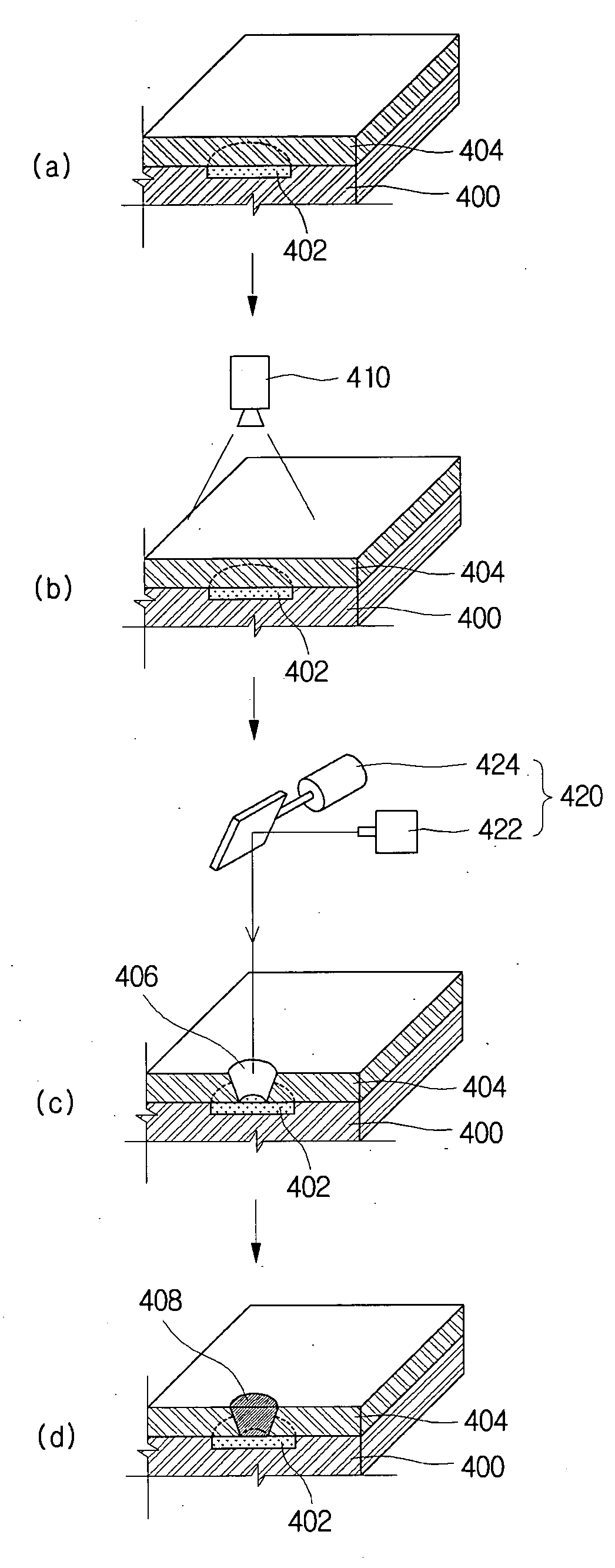
[0028]FIG. 3 is a diagram of printed circuit board manufa...


PUM

PropertyMeasurementUnit
Electrical conductoraaaaaaaaaa
Areaaaaaaaaaaa

Abstract

A printed circuit board manufacturing system and a manufacturing method thereof are disclosed. A method of manufacturing printed circuit board, comprising: providing a substrate that comprises a pad and an insulation layer covering the pad; acquiring an image of the substrate; acquiring location information of the pad by analyzing the image of the substrate; forming a via hole by removing a part of the insulation layer that corresponds the location information of the pad; and forming a via by filling the via hole with a conductive material, provides improved process conformity, even if the substrate has partial or nonlinear deformation, by considering the location information of the pad in the via hole forming. The improved conformity may allow more flexibility to substrate design and more integrity for circuitries on printed circuit board.

Description

CROSS-REFERENCE TO RELATED APPLICATIONS[0001]This application claims the benefit of Korean Patent Application No. 10-2007-0074788 filed with the Korean Intellectual Property Office on Jul. 25, 2007, the disclosure of which is incorporated herein by reference in its entirety.BACKGROUND[0002]1. Technical Field[0003]The present invention relates to a printed circuit board manufacturing system and a manufacturing method thereof.[0004]2. Description of the Related Art[0005]Miniaturization of electronic device is accomplished by miniaturization of electronic parts. Miniaturization of electronic parts does not mean minimized function. Electronic parts must have same functions in limited size. For this, researches for larger integrity have been accomplished.[0006]For larger integrity, structure of printed circuit board is improved from single-layered to multi-layered. Multi-layered printed circuit board may be manufactured by forming a circuit pattern substrate and then forming another circ...

Claims


Application Information

Patent Timeline
IPC IPC(8): H01B13/00B23K26/36B23K26/02B23K26/382H05K3/00
CPCH05K3/0008H05K1/0269H05K2201/09918H05K3/4679H05K2201/0108H05K3/0035Y10T29/49124H05K3/4644H05K3/42
Inventor CHO, CHUNG-WOOCHO, SOON-JINSEO, BYUNG-BAEYOO, KI-YOUNGAHN, SEOK-HWAN
Owner SAMSUNG ELECTRO MECHANICS CO LTD
Why Eureka
Try Eureka