Method for manufacturing printed circuit board

Active Publication Date: 2009-02-05
GARUDA TECH CO LTD
View PDF2 Cites 6 Cited by
  • Summary
  • Abstract
  • Description
  • Claims
  • Application Information

AI Technical Summary

Problems solved by technology

However, there is a cliff-like structure between the first dielectric layer and the conductive layer, creating gaps betwe

Method used


Image

  • Method for manufacturing printed circuit board
  • Method for manufacturing printed circuit board
  • Method for manufacturing printed circuit board

Examples


Example

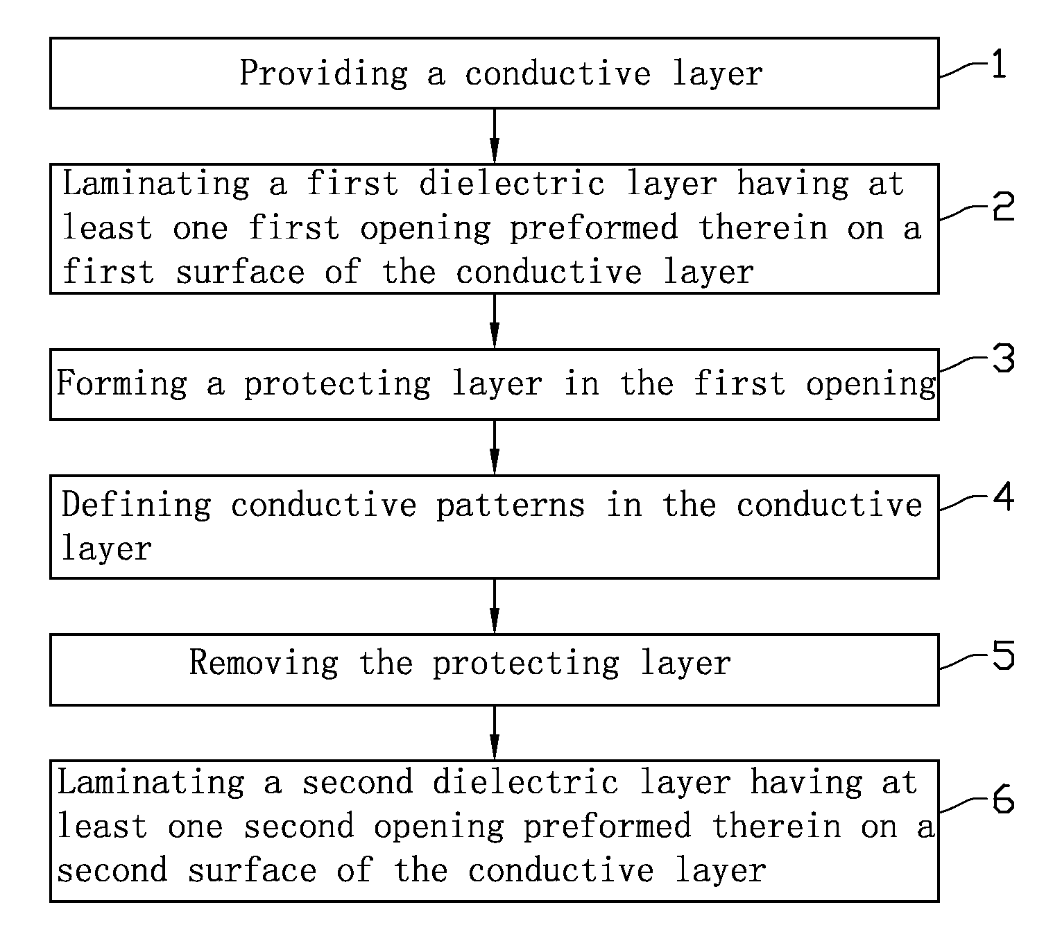
[0018]FIG. 1 illustrates a method for manufacturing a hollowed printed circuit and the method will be described more detail in accordance with the following preferred embodiment.

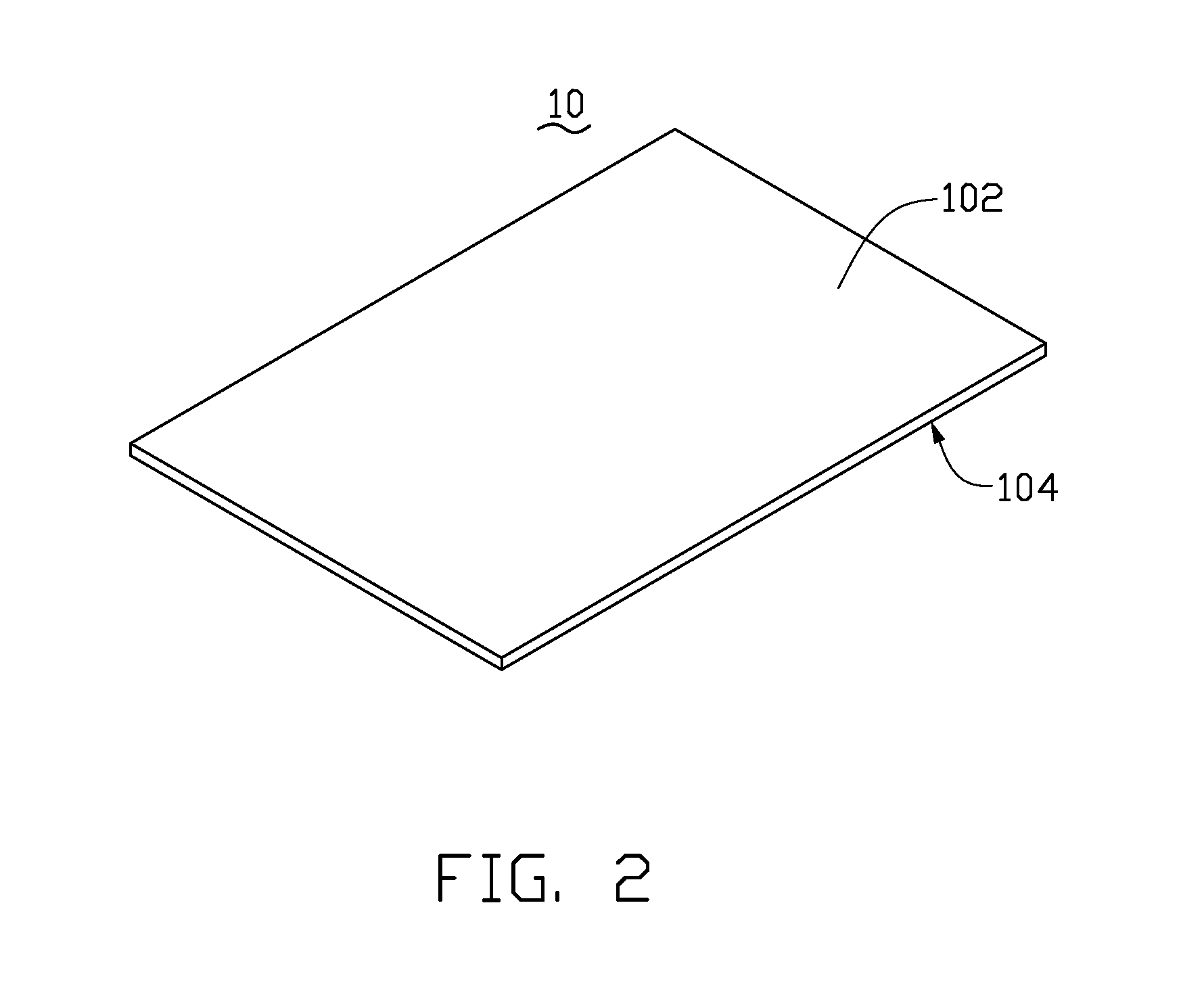
[0019]Referring to FIG. 2, a conductive layer 10 includes a first surface 102 and a second surface 104 opposite to the first surface 102. The conductive layer 10 can be made of a material having high electrical conductivity, such as copper, silver, etc. Advantageously, the conductive layer 10 can be processed using an acid solution such that a roughness of the first surface 102 and the second surface 104 is improved.

[0020]Referring to FIG. 3, a first dielectric layer 12 with two first openings 122 defined therein is shown. The first dielectric layer 12 can be made of a flexible material or a rigid material. Examples of the flexible material include polyimide, polyethylene terephtalate, polytetrafluoroethylene, polyamide, polymethylmethacrylate, polycarbonate, polyamide polyethylene-terephthalate copolymer an...


PUM

PropertyMeasurementUnit
Angleaaaaaaaaaa
Angleaaaaaaaaaa
Temperatureaaaaaaaaaa

Abstract

A method for manufacturing a hollowed printed circuit board includes steps of: providing an electrically conductive layer; laminating a first dielectric layer having a first through opening defined therein on a first surface of the electrically conductive layer; forming a protecting layer on the first surface of the electrically conductive layer in the first opening; creating an electrically conductive pattern in the conductive layer; removing the protecting layer; and laminating a second dielectric layer having a second through opening defined therein on an opposite second surface of the electrically conductive layer in a manner that the first through opening is aligned with the second through opening, thereby a portion of the electrically conductive layer is exposed to exterior through the first through opening and the second through opening.

Description

BACKGROUND[0001]1. Technical Field[0002]The present invention relates to a method for manufacturing a flexible printed circuit board and, particularly, to a method for manufacturing a multilayer flexible printed circuit board having different thicknesses in different areas.[0003]2. Discussion of Related Art[0004]Hollowed printed circuit boards are printed circuit boards that are hollowed. Two sides of the hollowed area are exposed to exterior thus the hollowed printed circuit board can provide electrical connection on the two sides.[0005]A method for manufacturing such a hollowed printed circuit board includes steps of: laminating a first dielectric layer having an opening preformed thereon on a first surface of a copper layer; forming conductive patterns in the copper layer; and laminating a second dielectric layer having an opening preformed thereon on a second surface of the copper layer, the two openings are aligned with each other thereby defining a hollowed area in the conduct...

Claims


Application Information

Patent Timeline
IPC IPC(8): H05K3/02H05K3/26H05K3/36
CPCH05K3/061H05K3/281H05K3/4092H05K2201/0397H05K2201/09063H05K2203/063Y10T29/49126Y10T29/49156Y10T29/49128Y10T29/49155Y10T29/49117Y10T29/49165H05K2203/308
Inventor HUANG, HSIAO-CHUNWU, MENG-HUNGLIN, CHENG-HSIEN
Owner GARUDA TECH CO LTD
Why Eureka
Try Eureka