Capacitive tactile tile sensor

a technology of tactile tile and sensor array, which is applied in the field of sensors, can solve the problems of unsuitable multi-curvature shapes such as robot fingers, other organic shapes, and unpliableness of sensors into different geometric shapes, and achieve the effect of increasing the ease of manufacturing and reliability of operation of the sensor array

Active Publication Date: 2009-02-05
PRESSURE PROFILE SYST
View PDF18 Cites 43 Cited by
  • Summary
  • Abstract
  • Description
  • Claims
  • Application Information

AI Technical Summary

Benefits of technology

[0015]Accordingly, it is an object of the present invention to overcome these and other drawbacks of the prior art by providing a novel capacitive tile tactile sensor designed to take advantage of the modern integrated circuits (IC). The novel tactile sensor is specifically adapted for ease and repeatability of high volume manufacturing.
[0016]It is another object of the present invention to provide a novel capacitive tile tactile sensor that can be consistently manufactured with large number of electrodes.
[0017]It is a further object of the present invention to provide a novel capacitive tile tactile sensor that can incorporate existing inexpensive ICs adapted to operate a limited number of individual sensors.
[0021]Dividing the entire plurality of sensors into such groups or tiles allows for substantial reduction of the number of interconnections required for the sensor operation and therefore increases the ease of manufacturing and reliability of operation of the sensor array.

Problems solved by technology

Notwithstanding that a substrate of Mylar® or of another dielectric material may be moderately flexible, at least for small deflections, the sensor so constructed remains substantially rigid and not pliable into different geometric shapes.
It is evident that these known devices are unsuitable for covering multi-curvature shapes such as a robot fingertip, other organic shapes, or to be incorporated in any object that must retain flexibility and pliability to conform to different shapes as a fabric.
For large tactile arrays having closely positioned electrodes, reliable and consistent manufacturing of such connections presents a technological challenge.
Despite the great extent of knowledge developed in the prior art, practical use of tactile conductive cloth-based sensor arrays has been limited until the present time.
This is caused by the difficulties in manufacturing the tactile sensor array with more than just a few electrodes.
Once the number of electrodes exceeds about 8 on each side of the array (the total of 16), direct attachment of the control unit wires to cloth-based electrodes becomes a burdensome procedure.
One great difficulty is managing the large number of wires on both sides of the tactile sensor array and connecting them repeatedly in a reliable manner without intermittent opens and shorts between wires or electrodes.
Another manufacturing difficulty associated with the prior art tactile sensors stems from the high pitch density sensor designs having electrodes located closely together, typically less than only about 3 mm apart.
Attaching individual wires to such electrodes becomes difficult as conductive epoxy or solder exhibits a tendency during assembly to deploy over more than one interconnection pad and therefore short the electrical connections.

Method used


Image

  • Capacitive tactile tile sensor
  • Capacitive tactile tile sensor
  • Capacitive tactile tile sensor

Examples


Embodiment Construction

[0033]A detailed description of the present invention follows with reference to accompanying drawings in which like elements are indicated by like reference letters and numerals.

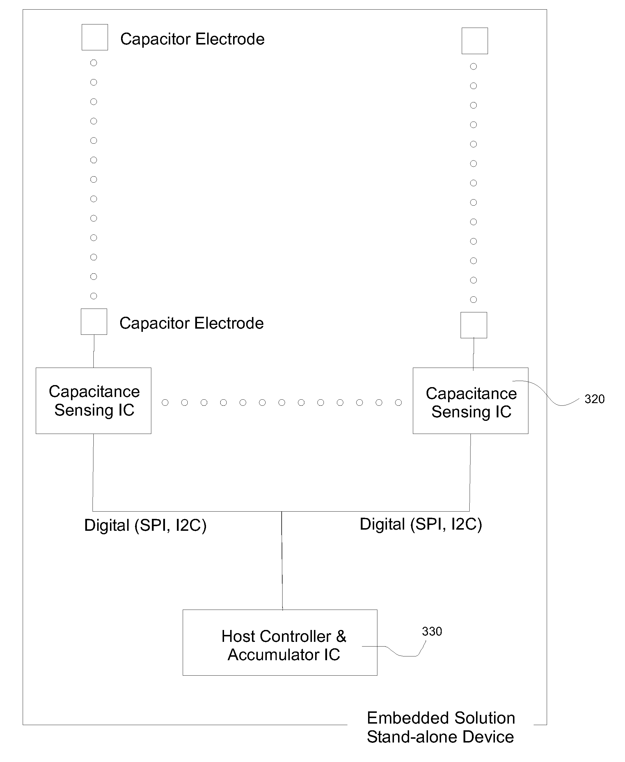
[0034]FIG. 3 shows a capacitive tile tactile sensor array according to the invention. It includes a top electrode ground layer 100 separated from the bottom sensing layer 300 by a compressible dielectric layer (not numbered). The top layer can be made from a conductive cloth, flex printed circuit, have a conductive metal surface formed thereon or be formed intermittently by a conductive object coming in contact with the sensor array from time to time.

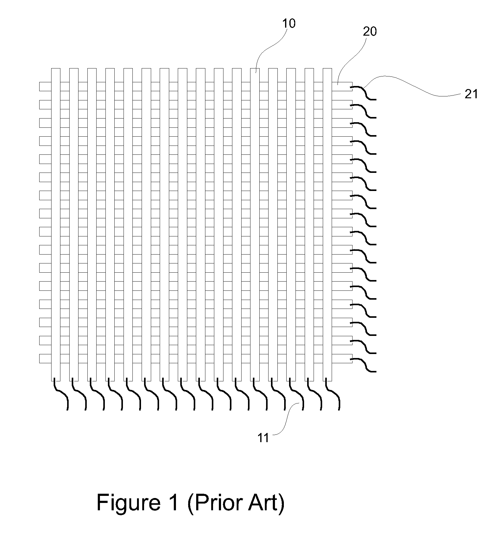
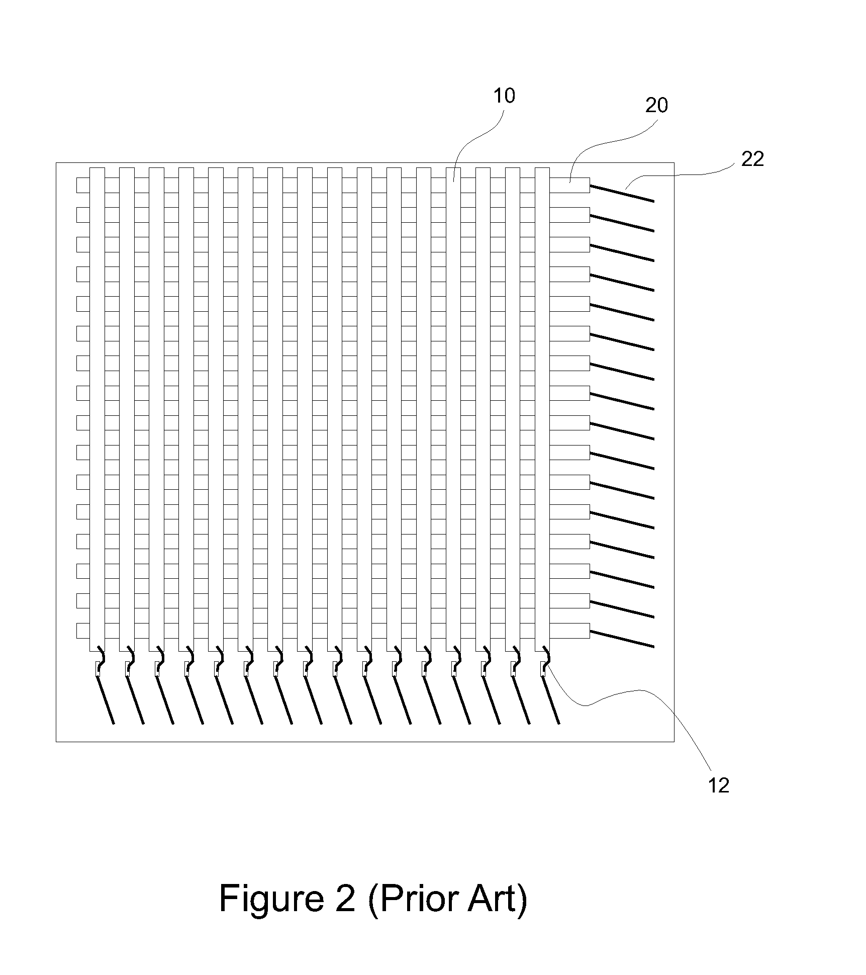
[0035]The bottom sensing layer contains an array of individual electrodes 301, each of these electrodes forming an individual sensor in combination with the top layer and a dielectric layer. These electrodes are divided into groups; in this example each vertical column forms one such group of electrodes, for example a fourth from the right column of electrodes i...


PUM


Abstract

A capacitive tile tactile sensor is described and includes several groups of individual sensors each controlled by a dedicated IC. Individual sensors are formed by sensing electrodes on one side of the sensor and a single ground electrode on the other side, the ground electrode is separated from the sensing electrodes by a compressible dielectric layer. A single electrical connection between the ground electrode and the sensing electrode layer allows for routing of all electrical connections including individual electrodes and a ground electrode to appropriate ICs within the same layer using conductive ink or other similar techniques. Stand-alone configurations are described as well as those adapted for communicating with outside control means including a personal computer. Arranging groups of sensors in parallel with each other creates a matrix of sensors while arranging them along a single line creates a linear strip sensor. Using off-the-shelf capacitance-sensing ICs to control a limited number of capacitance sensors allows reducing the number of electrical connections to the sensor array and increasing its reliability.

Description

CROSS-REFERENCE DATA[0001]This application is a continuation-in-part of a co-pending U.S. patent application Ser. No. 11 / 131,501 entitled “Hybrid Tactile Sensor” filed May 18, 2005, now U.S. Pat. No. 7,430,925. It is also a continuation-in-part of a co-pending U.S. patent application Ser. No. 11 / 407,535 entitled “Reconfigurable Tactile Sensor Input Device” filed Apr. 20, 2006, both documents incorporated herein in their entirety by reference.BACKGROUND OF THE INVENTION[0002]The present invention relates generally to a field of sensors, and, more particularly, to designs and methods of assembly of tactile array sensors used for sensing pressure distribution. Specifically, the present invention describes the use of multiple capacitance-sensing integrated circuits (ICs) each controlling a limited number of individual capacitor sensors, these individual sensors together forming the entire tactile array. This arrangement allows for convenient and repeatable manufacturing of tactile array...

Claims


Application Information

Patent Timeline
Patent Type & Authority Applications(United States)
IPC IPC(8): G01R27/26
CPCG01L5/228G01L1/146
Inventor SON, JAE S.ALFONSO, YERKO
Owner PRESSURE PROFILE SYST
Why Eureka
Try Eureka