

High-voltage mos transistor device
- Summary
- Abstract
- Description
- Claims
- Application Information
AI Technical Summary
Benefits of technology
Problems solved by technology
Method used
Image

Examples
first embodiment
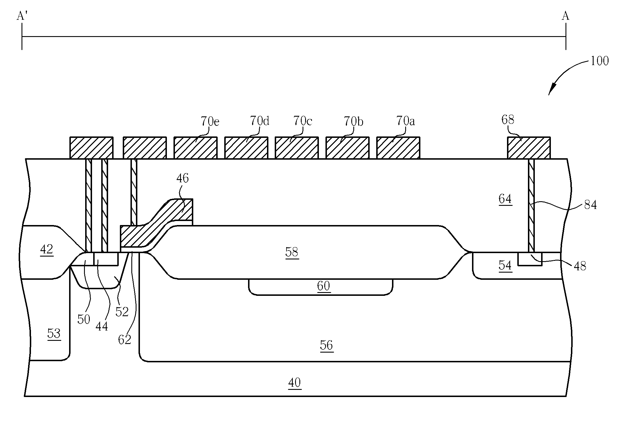
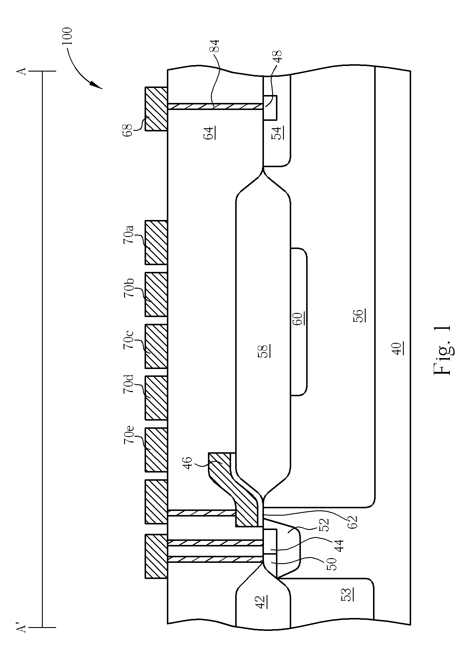
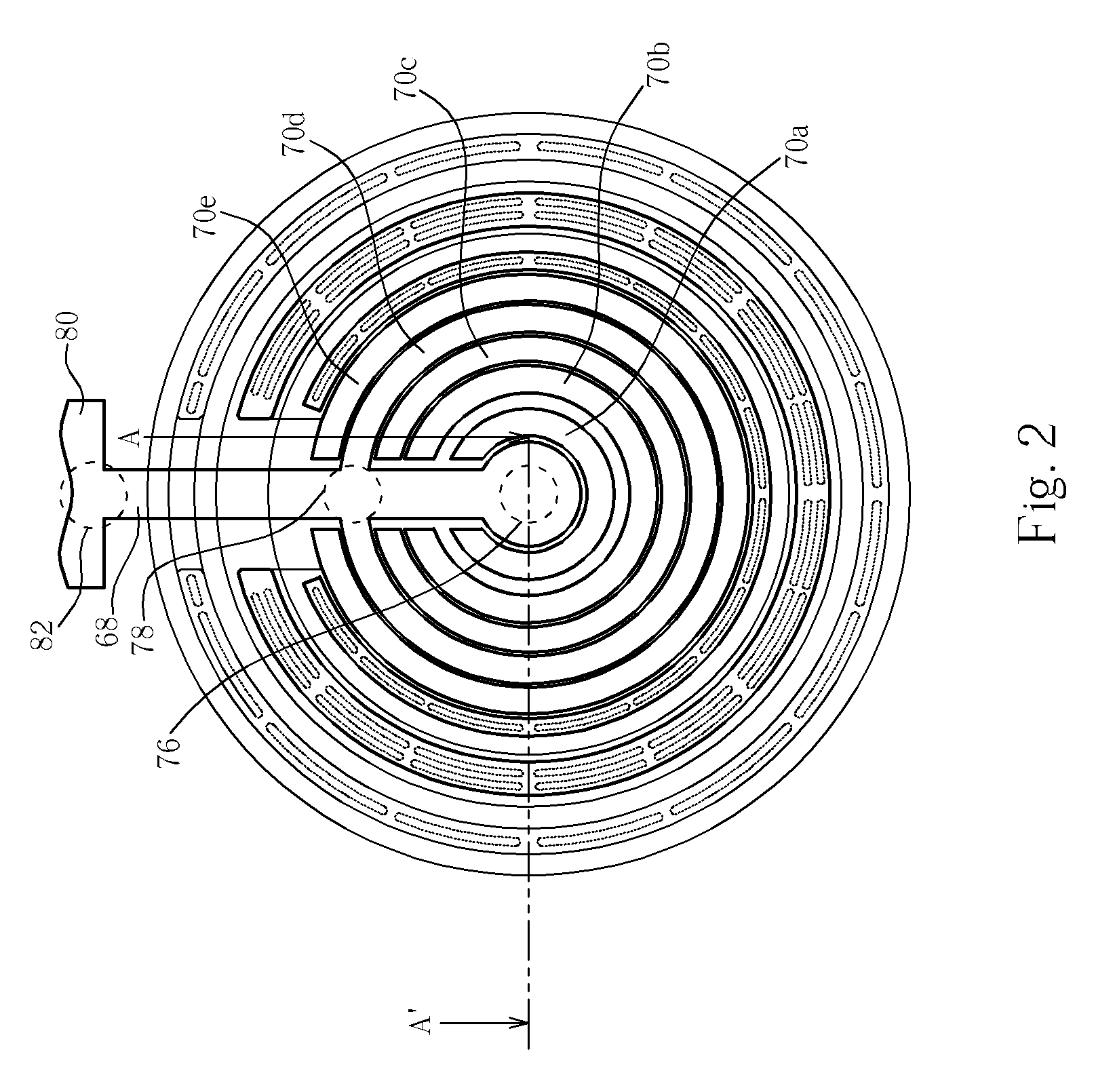
[0017]A high-voltage MOS transistor device according to the present invention will be described with reference to FIG. 1 and FIG. 2. FIG. 1 shows a cross-section diagram of the high-voltage MOS transistor device of the present invention. FIG. 2 shows a top view of the high-voltage MOS transistor device of the present invention, where the region between A and A′ in FIG. 1 corresponds to the region between A and A′ in FIG. 2. The high-voltage MOS transistor device 100 is formed on a substrate 40, such as a P doped silicon substrate, and the active area of the high-voltage MOS transistor device 100 is isolated by at least an isolation structure, such as a field oxide layer 42, or at least a shallow trench isolation (not shown). The high-voltage MOS transistor device 100 has a source 44, a gate 46, and a drain 48. The source 44 is a heavily N doped region and positioned next to a first heavily P doped region 50. Both the source 44 and the first heavily P doped region 50 are formed in a ...
fourth embodiment
[0022]Based on the spirit of the present invention, a fourth embodiment is disclosed with reference to FIG. 5 and FIG. 6, which are schematic diagrams of a plurality of first field plate rings 96a, 96b, 96c, 96d, 96e and a first conductive layer 94 of a high-voltage MOS transistor device. Other components of the high-voltage MOS transistor devices are the same as the prior embodiments. The field plate rings 96a-e are floating field plate rings. At least one of the floating field plate rings, such as the first field plate ring 96d in FIG. 6, is electrically connected to a first power supply 104. Therefore, a voltage from the first power supply 104 is applied to the first field plate ring 96d to decrease the electrical field near the PN junction next to the drain (not shown) and the PN junction next to the source (not shown). The value of the voltage may be equal to or less than that of the drain. Additionally, each of the floating first field plate rings 96a-e may be connected to a r...
PUM
 Abstract
Description
Claims
Application Information