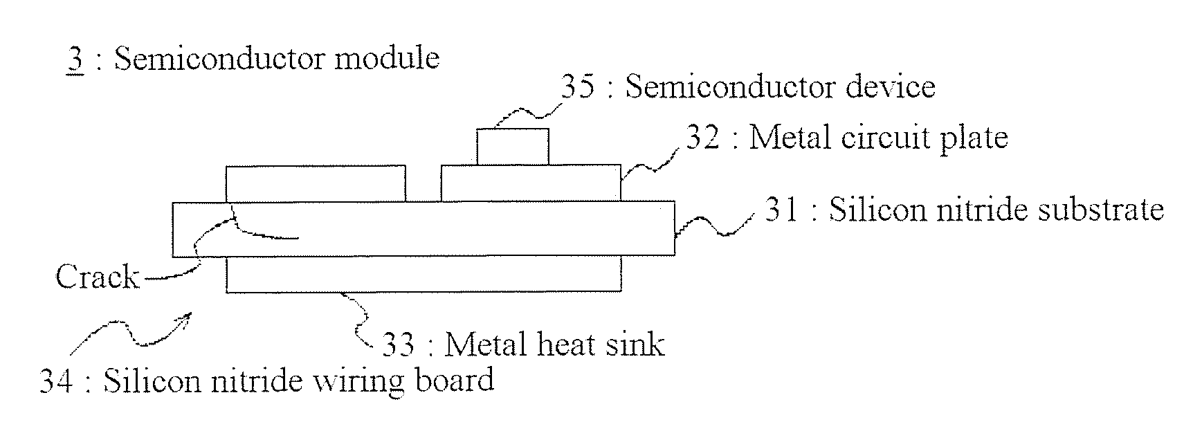
Silicon nitride substrate, a manufacturing method of the silicon nitride substrate, a silicon nitride wiring board using the silicon nitride substrate, and semiconductor module
a manufacturing method and silicon nitride technology, applied in the direction of solid-state devices, metal-working devices, domestic applications, etc., can solve the problems of low mechanical strength, low isolation voltage, cracking of ceramic substrates, etc., and achieve high fracture toughness, low thermal resistance, and high thermal conductivity
- Summary
- Abstract
- Description
- Claims
- Application Information
AI Technical Summary
Benefits of technology
Problems solved by technology
Method used
Image

Examples
examples
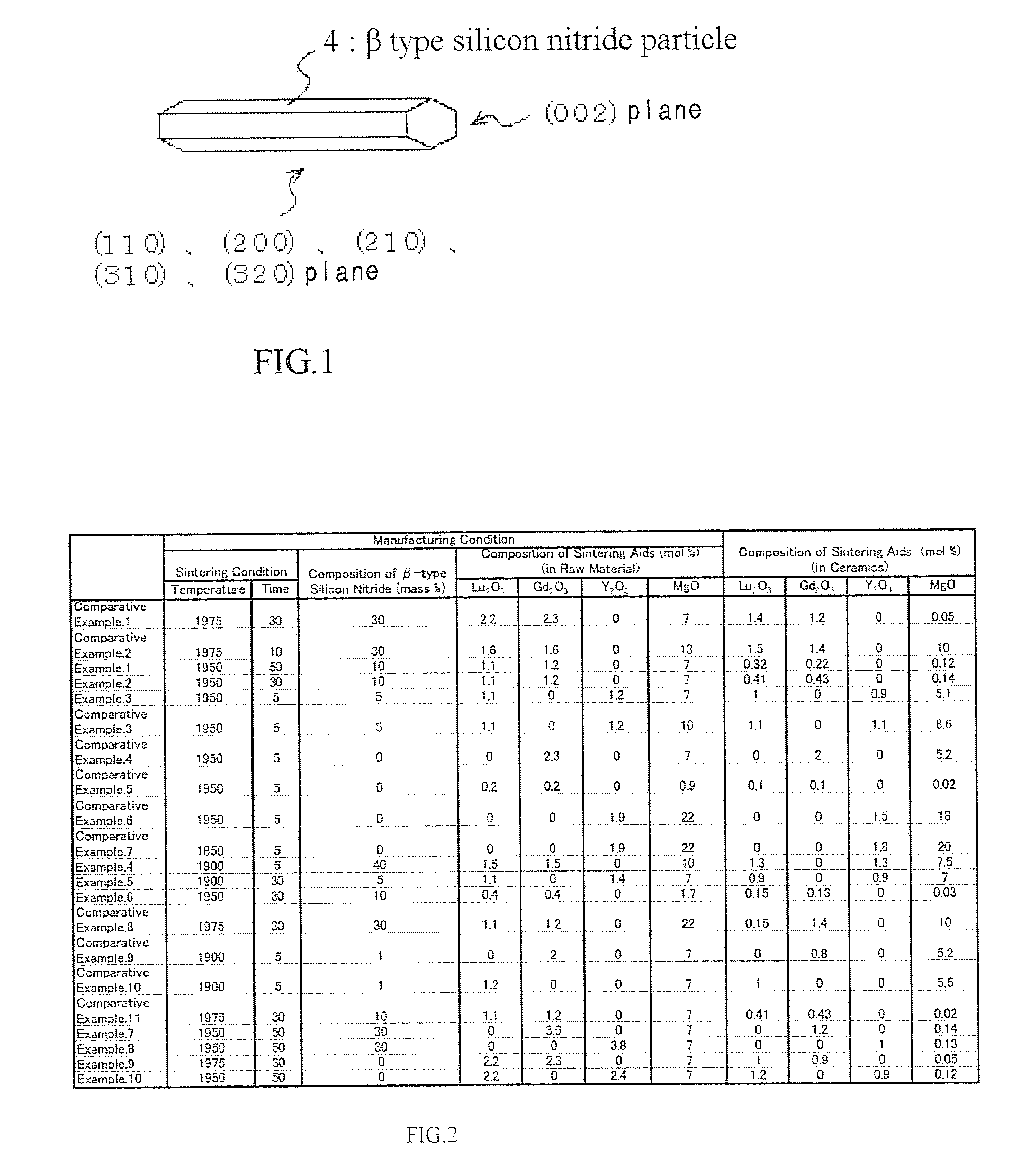
[0048]Hereafter, the example of this invention is described. However, this invention is not limited by these examples. Raw material powder of α type silicon nitride with average particle diameter of 0.7-1.2 micrometers, and oxygen amount of 0.5-2.0 mass % was prepared. Amounts shown in FIG. 2 of β type silicon nitride powder are mixed with the above mentioned raw material powder. In used β type silicon nitride powder, amount of oxygen was set to 0.5 mass % or less, mean particle diameter was set to 0.2-10 micrometers, and mean aspect ratio of particles was set to 10 or less. Degrees of in-plane orientation fa in the silicon nitride substrate obtained by above-mentioned condition were equivalent. Furthermore, by mixing MgO and Lu2O3, or Gd2O3, Y2O3 with the above mentioned powder by amounts of oxides shown in FIG. 2, starting materials were fabricated. After mixing 2 mass % of dispersing agent (trade name: Leoguard GP) with this starting material, each of the materials was put in the...
PUM
| Property | Measurement | Unit |
|---|---|---|
| Temperature | aaaaa | aaaaa |
| Time | aaaaa | aaaaa |
| Pressure | aaaaa | aaaaa |
Abstract
Description
Claims
Application Information
 - R&D Engineer
- R&D Manager
- IP Professional
- Industry Leading Data Capabilities
- Powerful AI technology
- Patent DNA Extraction
Browse by: Latest US Patents, China's latest patents, Technical Efficacy Thesaurus, Application Domain, Technology Topic.
© 2024 PatSnap. All rights reserved.Legal|Privacy policy|Modern Slavery Act Transparency Statement|Sitemap