Method For Utilizing Heavily Doped Silicon Feedstock To Produce Substrates For Photovoltaic Applications By Dopant Compensation During Crystal Growth
a technology of dopant compensation and crystal growth, which is applied in the direction of crystal growth process, polycrystalline material growth, and test/measurement of semiconductor/solid-state devices, etc., can solve the problems of high cost of purifying silicon, insufficient reduction of dopant atoms to an acceptable level, and high cost of purification silicon. achieve good solar cell performan
- Summary
- Abstract
- Description
- Claims
- Application Information
AI Technical Summary
Benefits of technology
Problems solved by technology
Method used
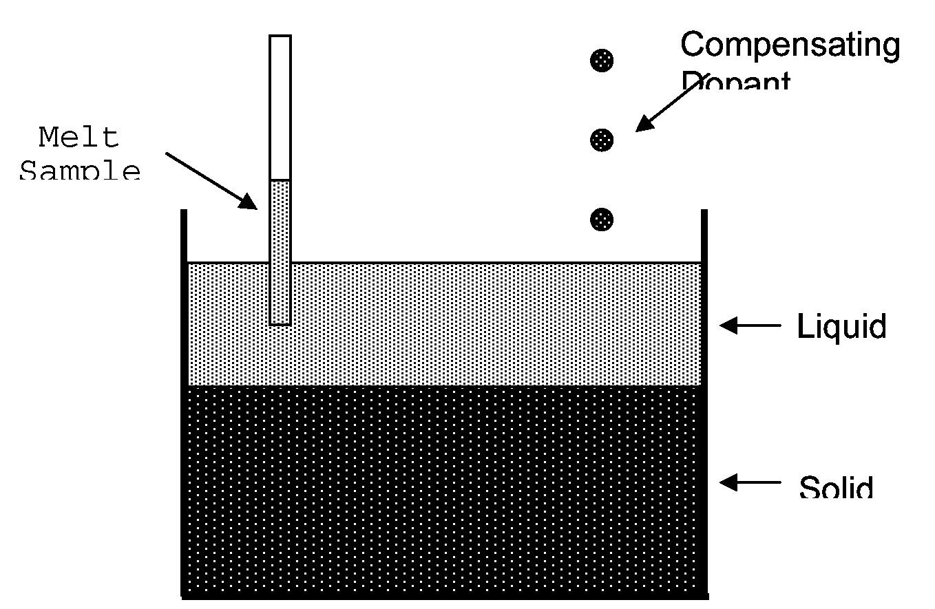
Image

Examples
example 1
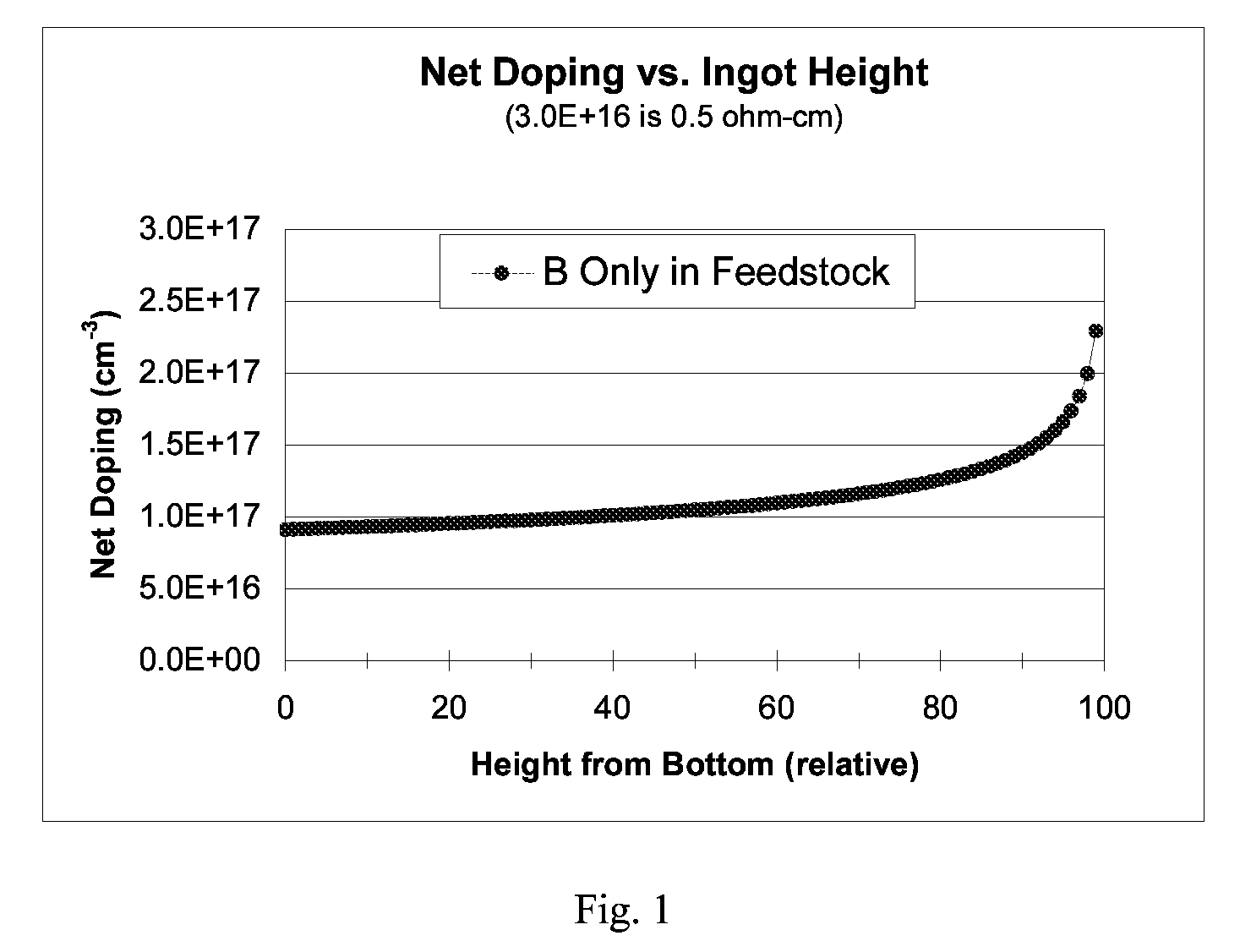
[0080]A candidate silicon feedstock, identified as “Brand A-6N,” was procured. A GDMS analysis indicated a very high concentration of boron and phosphorus, with boron at 4.6 ppmw (12.0 ppma or 6.0×1017 cm−3) and phosphorus at 15 ppmw (13.6 ppma or 6.8×1017 cm−3). Note that the boron concentration in the feedstock is 20 times the maximum value desired in the silicon crystal (3.0 ×1016 cm−3). Troublesome metals were generally below their respective GDMS detection limits, with V below 0.005 ppmw, Li, Ti, Mn, Co, Ni, Ag, and W all below 0.01 ppmw, S, Cu, Zn, Ga, As, Mo, Sb, and Pb all below 0.05 ppmw, and Cr below 0.1 ppmw. Only Fe and Al were detected at 0.06 ppmw and at 0.32 ppmw, respectively. A full-sized ingot (ID 060206-2), with a mass of 265 kg, was produced at Solar Power Industries in a DSS (directional solidification of silicon) furnace using 225 kg of the Brand A-6N feedstock and 40 kg of undoped silicon. FIG. 5 depicts the expected net doping in the ingot that was calculated...
example 2
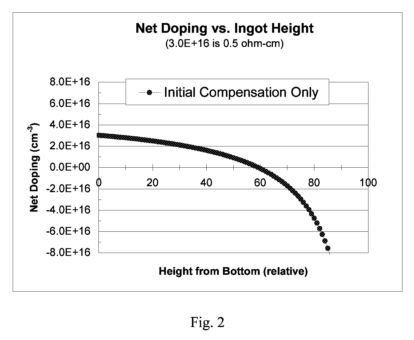
[0084]In order to demonstrate the benefits of dopant compensation in a controlled manner, a full-sized (265 kg) silicon ingot was produced using intrinsic silicon with boron added at a concentration of 0.5 ppmw (6.5×10¹⁶ B / cm3). This represented silicon feedstock which had a residual boron content at a level which may be obtained by some low-cost purification processes. With a segregation coefficient of 0.80, the expected boron concentration at the beginning (bottom) of a directionally-solidified ingot is 5.2×10¹⁶ B / cm3. This is almost twice the maximum level of 3.0×10¹⁶ B / cm3 desired in a substrate for solar cells, and which would increase as the crystal grows as the melt becomes more highly concentrated in boron. To bring the net doping concentration into the desired range for this simulated impure feedstock, the excess boron was compensated with arsenic in the initial silicon charge. The purpose was to demonstrate that feedstock that has a higher-than-desired dopant impurit...
example 3
[0091]In order to demonstrate the benefits of gallium dopant for N-Type silicon feedstock, a full-sized (265 kg) multi-crystalline silicon ingot was produced: 90.60 kg of N-Type silicon was charged with 174.40 kg prime semiconductor grade poly silicon raw material. The initial dopant concentration included 0.41 ppmw boron (5.74×10¹⁶ B / cm3) and 1.15 ppmw phosphorus (5.23×10¹⁶ P / cm3). Since gallium is a P-Type material, higher N-Type dopant concentration was required for testing purpose. Another 1.85 ppmw phosphorus (8.37×10¹⁶ P / cm3) in highly-doped wafers (0.002 Ωcm) shape was added to make the final charging silicon feedstock with 3.0 ppmw phosphorus (1.36×10¹⁷ P / cm3) of concentration.
[0092]For comparison, Chart 1 shows the net doping concentration from the bottom to the top of the ingot (boron concentration—phosphorus concentration) if the silicon ingot was cast without any other dopant addition. The entire ingot would be N-Type which would not be suitable for a substrate f...
PUM
 Abstract
Description
Claims
Application Information
 - R&D Engineer
- R&D Manager
- IP Professional
- Industry Leading Data Capabilities
- Powerful AI technology
- Patent DNA Extraction
Browse by: Latest US Patents, China's latest patents, Technical Efficacy Thesaurus, Application Domain, Technology Topic.
© 2024 PatSnap. All rights reserved.Legal|Privacy policy|Modern Slavery Act Transparency Statement|Sitemap