Stackable non-volatile resistive switching memory device and method

a resistive switching and memory device technology, applied in the direction of semiconductor devices, electrical devices, transistors, etc., can solve the problems of increasing power dissipation, non-scaling of sub-threshold slopes, and reducing device performan

Active Publication Date: 2012-02-23
INNOSTAR SEMICON SHANGHAI CO LTD
View PDF6 Cites 67 Cited by
  • Summary
  • Abstract
  • Description
  • Claims
  • Application Information

AI Technical Summary

Problems solved by technology

However, as field effect transistors (FET) approach sizes less than 100 nm, problems such as the short channel effect degrade device performance.
Moreover, such sub 100 nm device size can lead to sub-threshold slope non-scaling and also increases power dissipation.
These devices often require new materials and device structures to couple with silicon-based devices to form a memory cell, which lack one or more key attributes.
For example, Fe-RAM and MRAM devices have fast switching characteristics and good programming endurance, but their fabrication is not CMOS compatible and size is usually large.
Switching for a PCRAM device requires large amounts of power.
Organic RAM or ORAM is incompatible with large volume silicon-based fabrication and device reliability is usually poor.

Method used


Image

  • Stackable non-volatile resistive switching memory device and method
  • Stackable non-volatile resistive switching memory device and method
  • Stackable non-volatile resistive switching memory device and method

Examples


Embodiment Construction

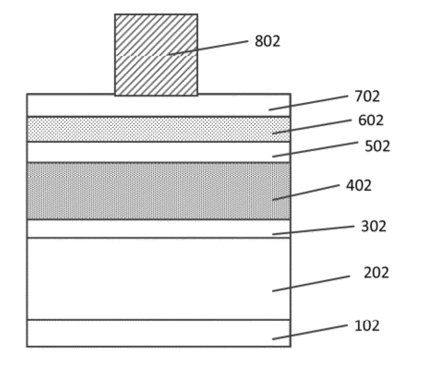
[0012]The present invention is generally related to resistive switching devices. More particularly, embodiments according to the present invention provide a method and a structure for forming a vertically stacked resistive switching device. The present invention can be applied to non-volatile memory devices but it should be recognized that the present invention can have a much broader range of applicability

[0013]The memory function of current non volatile memory devices are based on charges trapped in a dielectric material or a silicon floating gate. However, scaling of such charge-trap based materials is limited. For example, floating gate devices such as NOR or NAND devices have feature sizes of approximately 10 F2 and 4.5 F2, respectively, where F is the smallest feature size. Embodiments according to the present invention provide a method to form a non-volatile resistive switching device in layers which can be vertically stacked on top of one another to increase device density a...


PUM


Abstract

A method for forming a vertically stacked memory device. The method includes providing a semiconductor substrate having a surface region and forming a first dielectric material overlying the surface region. A first plurality of memory cells are formed overlying the first dielectric material. Each of the first plurality of memory cells includes at least a first top metal wiring structure spatially extending in a first direction, a first bottom wiring structure spatially extending in a second direction orthogonal to the first top metal wiring structure, and a first switching element sandwiched in an intersection region between the first top metal wiring structure and the first bottom metal wiring structure. In a specific embodiment, the method forms a thickness of second dielectric material overlying the first plurality of memory. A second plurality of memory cells are formed overlying the second dielectric material. Each of the second plurality of memory cells includes at least a second top metal wiring structure extending in the first direction, a second bottom wiring structure arranged spatially orthogonal to the second top metal wiring structure, and a second switching element sandwiched in an intersection region of the second top metal wiring structure and the second bottom metal wiring structure.

Description

CROSS REFERENCE TO RELATED APPLICATIONS[0001]Not ApplicableBACKGROUND[0002]The present invention is generally related to resistive switching devices. More particularly, embodiments according to the present invention provide a method and a structure for forming a stacked or vertically stacked resistive switching device. The present invention can be applied to non-volatile memory devices but it should be recognized that the present invention can have a much broader range of applicability[0003]The success of semiconductor devices has been mainly driven by an intensive transistor down-scaling process. However, as field effect transistors (FET) approach sizes less than 100 nm, problems such as the short channel effect degrade device performance. Moreover, such sub 100 nm device size can lead to sub-threshold slope non-scaling and also increases power dissipation. It is generally believed that transistor-based memories such as those commonly known as Flash may approach an end to scaling w...

Claims


Application Information

Patent Timeline
Patent Type & Authority Applications(United States)
IPC IPC(8): H01L29/68H01L21/336
CPCH01L45/16H01L27/2481H01L45/122H01L45/148H01L45/04H10B63/84H10N70/245H10N70/826H10N70/884H10N70/011H10B63/80H10B63/30H10N70/20H10N70/821H10N70/841
Inventor HERNER, SCOTT BRAD
Owner INNOSTAR SEMICON SHANGHAI CO LTD
Why Eureka
Try Eureka