Wiring substrate and display device including the same

Inactive Publication Date: 2009-02-12
SHARP KK
13 Cites 29 Cited by

AI-Extracted Technical Summary

Problems solved by technology

However, it is difficult to hold the pressure bonding stage and the pressure bonding tool completely parallel to each other, and the pressure bonding stage and the pressure bonding tool are usually somewhat tilted with respect to each other in the heat pressure bonding process.
In this case, the pressure is not uniformly applied between each terminal portion and bump elec...

Method used

[0078]The liquid crystal display device of the first preferred embodiment has the support member 90 that is in contact with both the active matrix substrate 10 and the driving IC chip 50. Therefore, the driving IC chip 50 can be mounted with high reliability. The reason for this will now be described in detail with reference to FIGS. 6A, 6B, and 6C.
[0081]The support member 90 preferably has an insulating property. In the case where the support member 90 is electrically conductive, short-circuiting may occur between the terminal portions 14a, between the terminal portion 14a and the bump electrode 51, and the like through the electrically conductive fine particles 61 dispersed in the anisotropic electrically conductive layer 60 and the support member 90. As a result, a leakage current may be generated. By using the support member 90 having an insulating property, such short-circuiting caused by the support member 90 can be prevented and generation of leakage current can be effectively suppressed.
[0092]As shown in FIG. 9, a support member 90 having a substantially rectangular cylindrical shape may be provided in the central region of the driving IC chip 50, that is, the region that does not have the bump electrodes 51 and is not in contact with the wirings 14. This structure can eliminate non-uniformity of pressure application resulting from warping and deformation of the active matrix substrate 10 in a preferable manner.
[0093]In this case, the support member 90 may further be provided between at least a portion of the periphery of the driving IC chip 50 and the active matrix substrate 10 as shown in FIGS. 3, 7, and 8. This structure can eliminate non-uniformity of pressure application resulting from the tilt between the pressure bonding stage and the pressure bonding tool and non-uniformity of pressure application resulting from warping and deformation of the active matrix substrate 10 in a preferable manner.
[0099]However, providing the insulating member 70 between adjacent terminal portions 14a as in the second preferred embodiment can effectively suppress generation of leakage current resulting from a short-circuit between adjacent wirings 14, between adjacent bump electrodes 51, or between the wiring 14 and the bump electrode 51.
[0100]The insulating member 70 may be arranged entirely along a portion of each wiring 14 that is in contact with the anisotropic electrically conductive layer 60. The terminal portion 14a is wider than the portion other than the terminal portion 14a of the wiring 14. Therefore, the space between each terminal portion 14a and a wiring 14 adjacent to that terminal portion 14a is relatively narrow. Therefore, for example in the case where the insulating member 70 is not provided, a leakage current is likely to be generated between a terminal portion 14a and a wiring 14 adjacent to the terminal portion 14a. In the second preferred embodiment, however, as shown in FIG. 10, the insulating member 70 is provided in the relatively narrow space between each terminal portion 14a and a wiring 14 adjacent to that terminal portion 14a. Therefore, generation of leakage current can be effectively suppressed.
[0101]As shown in FIG. 11, the insulating member 70 preferably has an approximately trapezoidal shape in cross section. In order to effectively suppress generation of leakage current, the top surface of the insulating member 70 preferably has a narrow width. More preferably, the width of the top surface of the insulating member 70 is equal to or less than the particle size (more specifically, mean particle size) of the electrically conductive fine particles 61.
[0102]In order to effectively suppress generation of leakage current, the top surface of the insulating member 70 is preferably in contact with the driving IC chip 50. However, the top surface of the insulating member 70 need not necessarily be in contact with the driving IC chip 50. As shown in FIG. 11, there may be a gap between the insulating member 70 and the driving IC chip 50. Even when there is a gap between the insulating member 70 and the driving IC chip 50, generation of leakage current can be suppressed as compared to the case where the insulating member 70 is not provided. The gap between the insulating member 70 and the driving IC chip 50 is preferably equal to or less than the particle size (more specifically, mean particle size; e.g., about 3 μm to about 5 μm, for example) of the electrically conductive fine particles 61. With this structure, the electrically conductive fine particles 61 can be effectively prevented from being disposed between the insulating member 70 and the driving IC chip 50. In this case, the height of the insulating member 70 is shown by, e.g., the following formula I, where H is the height of the insulating member 70, h1 is the cell gap of the liquid crystal layer 40, h2 is the height of the bump electrode 51, h3 is the height of the terminal portion 14a, r is the particle size of the electrically conductive fine particles 61, and A is the oblateness of the electrically conductive fine particles 61:
[0105]In the case where the anisotropic electrically conductive layer 60 is formed by a wet process, it is preferable to apply a liquid repellent property (a property to repel ink for forming the anisotropic electrically conductive layer 60) to the surface of the insulating member 70. This can effectively suppress short-circuiting between the wirings 14, between the bump electrodes 51, or between the wiring 14 and the bump electrode 51, and therefore can effectively suppress generation of leakage current.
[0109]As shown in FIGS. 12 and 13, adjacent insulating members 70 may be connected together so as to extend across the wiring 14. This structure can more effectively suppress generation of leakage current between a terminal portion 14a and a wiring 14 adjacent to the terminal portion 14a.
[0112]Bump electrodes 51 are linearly arranged in line along the direction of the longer side of the driving IC chip 50 (the width direction of the terminal portions 14a). The terminal portion 14a is wider than the portion other than the terminal portion 14a of the wiring 14. Therefore, in the fifth modification, the space between adjacent terminal portions 14a is relatively narrow, while the space between the portions other than the terminal portions 14a of the wirings 14 and the space between the portion other than the terminal portion 14a of each wiring 14 and an adjacent terminal portion 14a are relatively wide. Therefore, in this structure, generation of leakage current can be effectively suppressed by providing the insulating member 70 between the terminal portions 14a as shown in FIG. 14.
[0114]As shown in FIG. 16, an insulating layer 100 may be formed on the surface of the periphery of the active matrix substrate 10. The insulating layer 100 covers the wirings 14 and has openings 100a that expose the terminal portions 14a. This structure can very effectively suppress short-circuiting between the wirings 14.
[0117]In the second preferred embodiment, the insulating member 70 is provided between adjacent wirings 14 o...

Benefits of technology

[0012]In order to overcome the problems described above, preferred embodiments of the present...

Abstract

An active matrix substrate includes a first substrate and a driving integrated circuit chip mounted on the first substrate. A support member is provided between the active matrix substrate and the driving IC chip so as to be in contact with both the active matrix substrate and the driving IC chip.

Application Domain

Final product manufactureSemiconductor/solid-state device details +5

Technology Topic

Integrated circuitEngineering +2

Image

  • Wiring substrate and display device including the same
  • Wiring substrate and display device including the same
  • Wiring substrate and display device including the same

Examples

  • Experimental program(1)

Example

[0065]Hereinafter, preferred embodiments of the present invention will be described in detail with reference to the figures.
First Preferred Embodiment
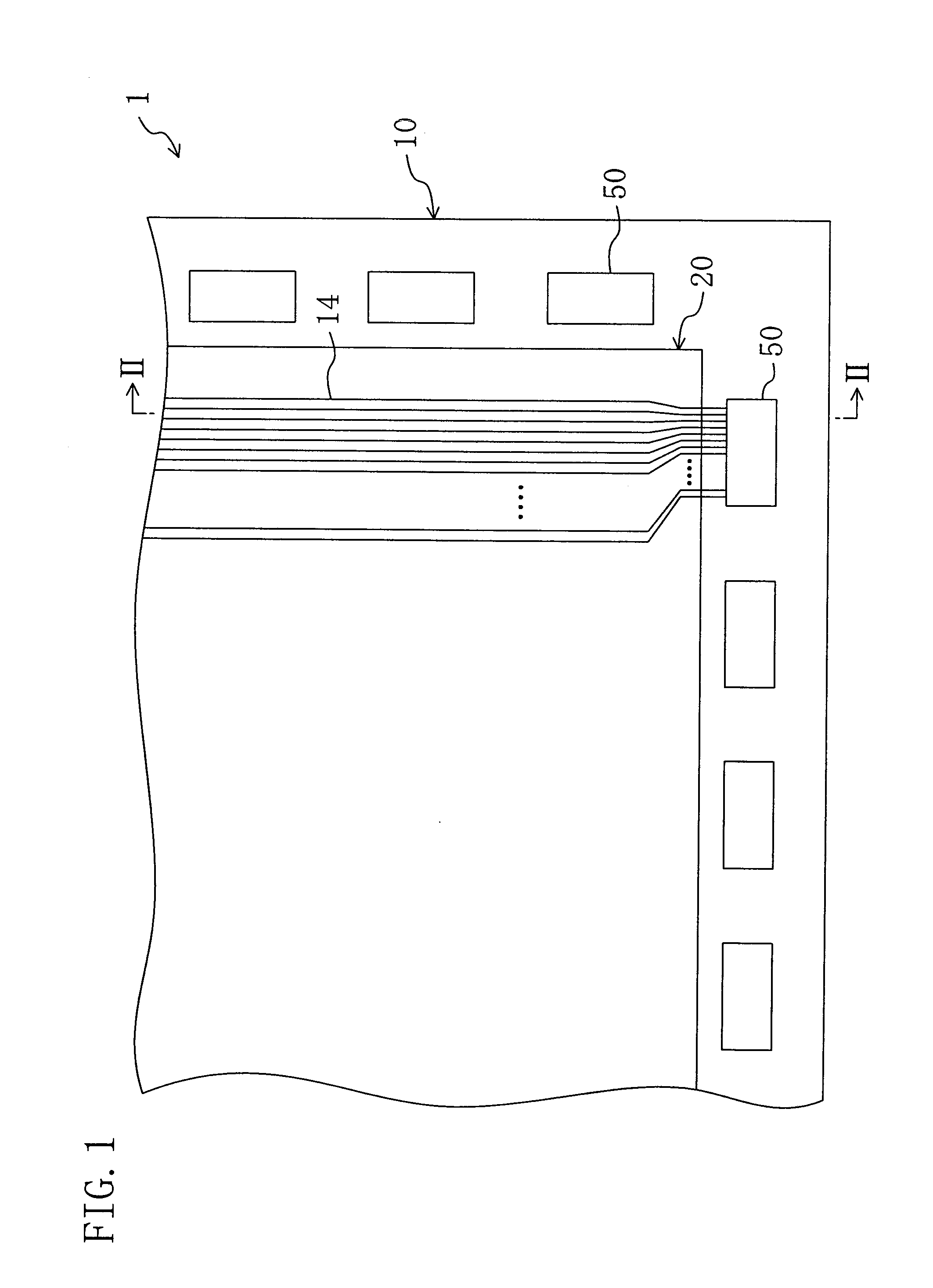
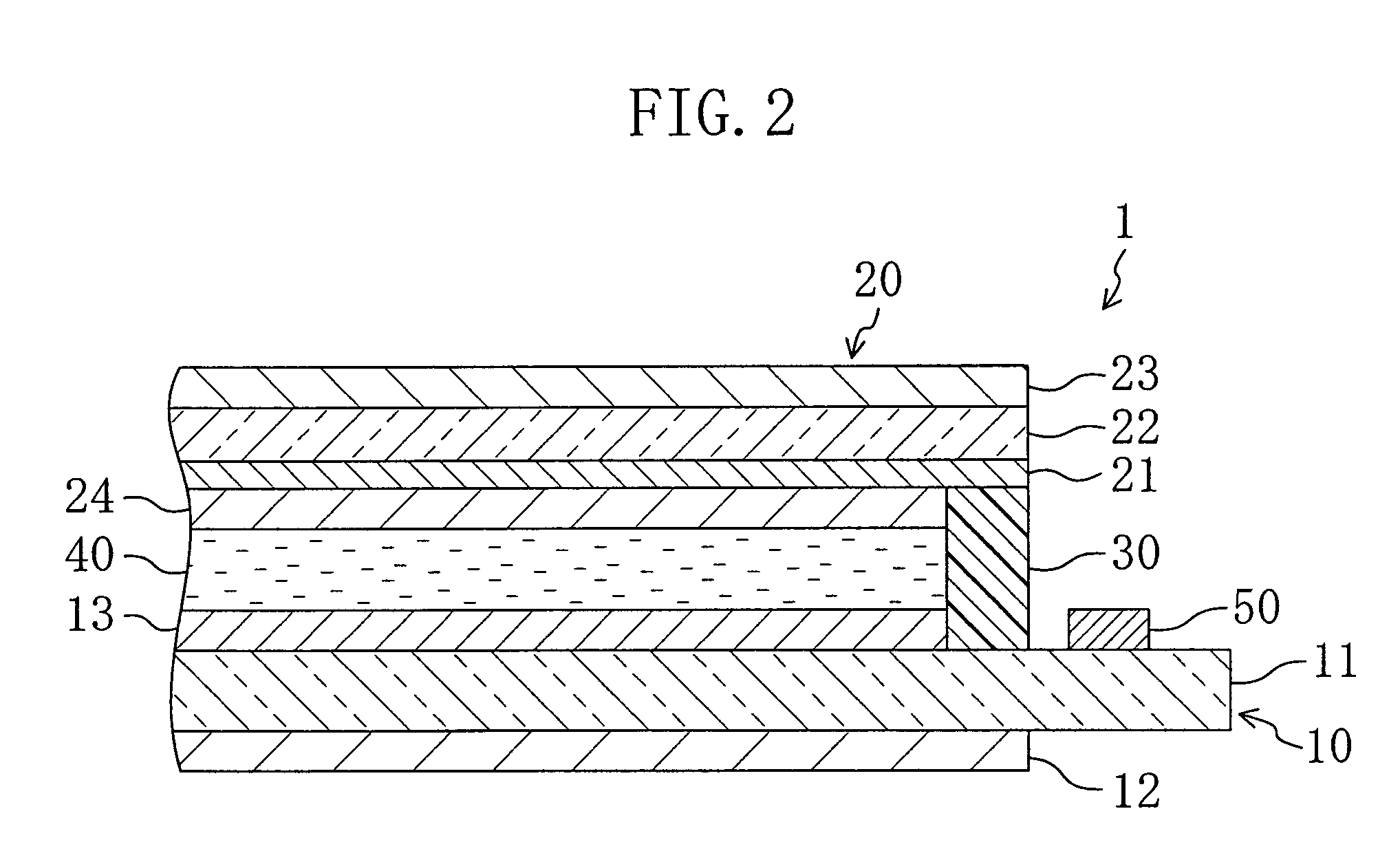
[0066]FIG. 1 is a plan view of a liquid crystal display device 1 according to a first preferred embodiment of the present invention. FIG. 2 is a cross-sectional view taken along line II-II in FIG. 1.
[0067]The liquid crystal display device 1 according to the first preferred embodiment preferably includes an active matrix substrate 10, a counter substrate 20 facing the active matrix substrate 10, a liquid crystal layer 40 interposed between the active matrix substrate 10 and the counter substrate 20 as a display medium layer, and a seal member 30 bonding the active matrix substrate 10 and the counter substrate 20 to each other and sealing the liquid crystal layer 40.
[0068]The active matrix substrate 10 has a first substrate 11 made of plastic or glass and a first polarizing plate 12 provided on the opposite side to the liquid crystal layer 40 on the first substrate 11. A plurality of gate lines and a plurality of source lines are provided on the active matrix substrate 10. The plurality of gate lines extend in parallel or substantially in parallel with each other and the plurality of source lines extend in parallel or substantially in parallel with each other at an angle (typically at a right angle) to the extending direction of the gate lines (in this specification, electrode lines such as the gate lines and the source lines are collectively referred to as “wirings”14). A switching element (not shown) such as a TFT (Thin Film Transistor) element is provided near each intersection of the gate lines and the source lines. Each switching element is electrically connected to a corresponding gate line and a corresponding source line. A plurality of pixel electrodes 13 are arranged in a prescribed pattern (typically, in a matrix pattern) on the surface of the active matrix substrate 10 located on the side of the liquid crystal layer 40. Each pixel electrode 13 is electrically connected to a corresponding switching element (not shown) and is driven by that switching element.
[0069]The counter substrate 20 has a second substrate 22, a second polarizing plate 23 provided on the opposite side to the liquid crystal layer 40 on the second substrate 22, and an upper common electrode 21 provided on the surface of the second substrate 22 on the side of the liquid crystal layer 40. The liquid crystal display device 1 is driven by a voltage that is applied to the liquid crystal layer 40 by the upper common electrode 21 and the plurality of pixel electrodes 13 provided on the active matrix substrate 10.
[0070]In the first preferred embodiment, the active matrix substrate 10 and the counter substrate 20 preferably have a substantially rectangular shape and the active matrix substrate 10 is larger than the counter substrate 20. The counter substrate 20 covers the liquid crystal layer 40 on the active matrix substrate 10. Driving integrated circuit chips (hereinafter, sometimes referred to as “driving IC chips”) 50 are preferably bare-chip mounted on the periphery of the active matrix substrate 10 which is not covered by the counter substrate 20.
[0071]FIG. 3 is an enlarged plan view of a region around a driving IC chip 50.
[0072]FIG. 4 is a cross-sectional view taken along line IV-IV in FIG. 3.
[0073]As shown in FIGS. 3 and 4, the driving IC chip 50 as an integrated circuit chip has a plurality of bump electrodes 51 as input/output terminals. The bump electrodes 51 are arranged in a staggered pattern along the direction of the longer side of the driving IC chip 50 (the width direction of terminal portions 14a). The bump electrodes 51 function also as bonding bump electrodes. The bump electrodes 51 are respectively electrically connected through an anisotropic electrically conductive layer 60 to the terminal portions 14a of the wirings 14 provided on the periphery of the active matrix substrate 10. The anisotropic electrically conductive layer 60 is made of an insulating resin with electrically conductive fine particles 61 dispersed therein.
[0074]In the liquid crystal display device 1 of this preferred embodiment, a support member 90 is provided in contact with the driving IC chip 50 and the active matrix substrate 10. More specifically, the support member 90 is preferably shaped like a wall and extends as a band so as to surround the driving IC chip 50.
[0075]FIGS. 5A and 5B are schematic cross-sectional views illustrating a mounting process in the case where the support member 90 is not provided. FIG. 5A is a schematic cross-sectional view of the state before application of pressure. FIG. 5B is a schematic cross-sectional view of the state when mounting is completed.
[0076]Essentially, it is preferable that a pressure bonding stage 8 and a pressure bonding tool 9 are completely parallel to each other. However, it is difficult to hold the pressure bonding stage 8 and the pressure bonding tool 9 completely parallel to each other, and the pressure bonding stage 8 and the pressure bonding tool 9 are usually somewhat tilted with respect to each other as shown in FIG. 5A. In this state, the pressure is not uniformly applied to each terminal portion 14a. An excessive pressure is applied to a region where the active matrix substrate 10 and the driving IC chip 50 are relatively close to each other (a region on the left side of FIGS. 5A and 5B), while the pressure that is applied to a region where the active matrix substrate 10 and the driving IC chip 50 are relatively far from each other (a region on the right side of FIGS. 5A and 5B) is not enough to electrically connect the terminal portions 14a to the respective bump electrodes 51. In other words, in order to obtain electrical conduction between the terminal portions 14a and the bump electrodes 51, the electrically conductive fine particles 61 need to be pressed by the terminal portions 14a and the bump electrodes 51 enough to be flatten (deformed) to some extent. However, the pressure that is applied to the region on the right side of FIGS. 5A and 5B is not large enough to deform the electrically conductive fine particles 61.
[0077]Therefore, as shown in FIG. 5B, the terminal portions 14a and the bump electrodes 51 may be deformed, disconnected, and the like in the region on the left side of the figure due to the excessive pressure. Moreover, the terminal portions 14a and the bump electrodes 51 may not be electrically connected in a preferable manner in the region on the right side of the figure due to the insufficient pressure. Therefore, mounting may not be implemented in a preferable manner.
[0078]The liquid crystal display device of the first preferred embodiment has the support member 90 that is in contact with both the active matrix substrate 10 and the driving IC chip 50. Therefore, the driving IC chip 50 can be mounted with high reliability. The reason for this will now be described in detail with reference to FIGS. 6A, 6B, and 6C.
[0079]FIGS. 6A, 6B, and 6C are schematic cross-sectional views illustrating a mounting process in the first preferred embodiment. More specifically, FIG. 6A is a schematic cross-sectional view of the state before application of pressure. FIG. 6B is a schematic cross-sectional view of the state during application of pressure. FIG. 6C is a schematic cross-sectional view of the state when mounting is completed.
[0080]In the first preferred embodiment, even when the pressure bonding stage 8 and the pressure bonding tool 9 are somewhat tilted with respect to each other, the support member 90 that is taller than the terminal portions 14a corrects the parallelism between the pressure bonding stage 8 and the pressure bonding tool 9 to some extent, as shown in FIG. 6B. More specifically, as shown in FIG. 6B, when a portion of the support member 90 contacts the active matrix substrate 10, reaction force is applied to the pressure bonding tool 9 through that portion of the support member 90. Therefore, the tilt of the pressure bonding tool 9 with respect to the pressure bonding stage 8 is reduced and the pressure is relatively uniformly applied to each terminal portion 14a. As a result, the driving IC chip 50 can be mounted with high reliability.
[0081]The support member 90 preferably has an insulating property. In the case where the support member 90 is electrically conductive, short-circuiting may occur between the terminal portions 14a, between the terminal portion 14a and the bump electrode 51, and the like through the electrically conductive fine particles 61 dispersed in the anisotropic electrically conductive layer 60 and the support member 90. As a result, a leakage current may be generated. By using the support member 90 having an insulating property, such short-circuiting caused by the support member 90 can be prevented and generation of leakage current can be effectively suppressed.
[0082]In the first preferred embodiment, the support member 90 is arranged so that the outer edge thereof protrudes from the periphery of the driving IC chip 50 in view of an alignment margin. With this structure, the support member 90 can be reliably placed on the periphery of the driving IC chip 50 even when the driving IC chip 50 is misaligned with respect to the support member 90.
[0083]Hereinafter, a manufacturing process of the liquid crystal display device 1 of the first preferred embodiment, especially a manufacturing process of the support member 90 and a mounting process of the driving IC chip 50, will be described in detail.
[0084]First, various wirings 14 such as gate lines and source lines, TFTs, pixel electrodes 13, and the like are formed on the first substrate 11. The support member 90 is then formed. The support member 90 can be formed by forming an insulating resin film by a wet process such as a screen printing method and patterning the insulating film by a patterning technology such as a photolithography technology. The height of the support member 90 may be in the range of about 5 μm to about 25 μm (e.g., about 10 μm), for example. For example, the support member 90 is preferably made of an acrylic resin, a novolac resin, a polyimide resin, an epoxy resin, and the like. The periphery of the active matrix substrate 10 is then bonded to the periphery of the counter substrate 20 by the seal member 30 to form a space (an empty cell) for injection of a liquid crystal material. Thereafter, a liquid crystal material is injected (e.g., vacuum-injected) into the space (the empty cell) to form the liquid crystal layer 40.
[0085]The driving IC chip 50 is then mounted. More specifically, by a wet process such as an ink-jet method, the anisotropic electrically conductive layer 60 is formed on the periphery of the active matrix substrate 10 where the driving IC chip 50 is to be mounted. The driving IC chip 50 is then placed thereon and aligned. In this state, the active matrix substrate 10 is placed on a flat pressure bonding stage and the driving IC chip 50 is heated and pressed with a heated pressure bonding tool. The liquid crystal display device 1 is completed by thus mounting the driving IC chip 50.
[0086]In the case where a wet process is used to form the anisotropic electrically conductive layer 60, it is preferable to apply a liquid repellent property (a property to repel ink for forming the anisotropic electrically conductive layer 60) to the surface of the support member 90 in advance.
First Modification
Modification of the First Preferred Embodiment
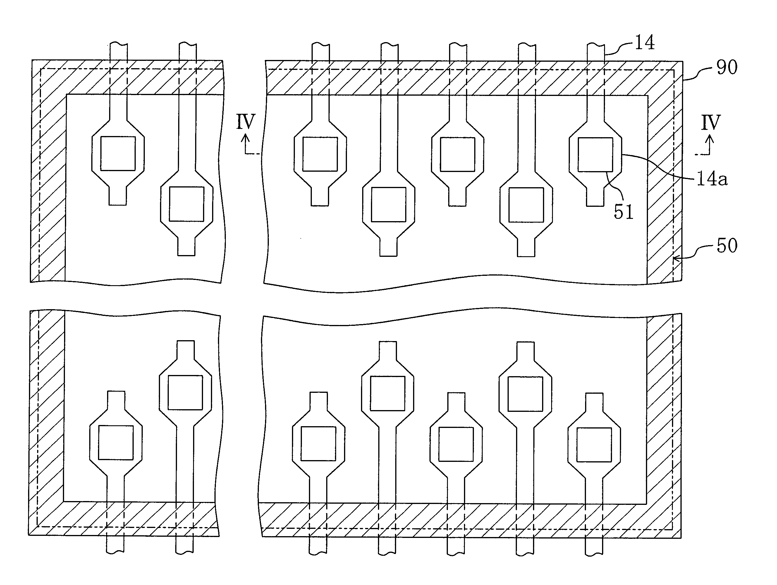
[0087]FIG. 7 is an enlarged plan view of a region around a driving IC chip 50 of a liquid crystal display device according to a first modification of the first preferred embodiment of the present invention.
[0088]As shown in FIG. 7, a support member 90 having a substantially rectangular cylindrical shape may be provided between each of the four corners of the driving IC chip 50 and the active matrix substrate 10. With this structure, the support member 90 does not overlap the wirings 14 and unnecessary pressure application to the wirings 14 can be suppressed.
Second Modification
Modification of the First Preferred Embodiment
[0089]FIG. 8 is an enlarged plan view of a region around a driving IC chip 50 of a liquid crystal display device according to a second modification. For convenience of explanation, bump electrodes 51 and wirings 14 are not shown in FIG. 8.
[0090]As shown in FIG. 8, the support member 90 may be provided between at least a portion of the periphery of the driving IC chip 50 and the active matrix substrate 10. With this structure, the support member 90 can be prevented from inhibiting the flow of an insulating resin during formation of the anisotropic electrically conductive layer 60.
Third Modification
Modification of the First Preferred Embodiment
[0091]FIG. 9 is an enlarged plan view of a region around a driving IC chip 50 of a liquid crystal display device according to a third modification. For convenience of explanation, bump electrodes 51 and wirings 14 are not shown in FIG. 9.
[0092]As shown in FIG. 9, a support member 90 having a substantially rectangular cylindrical shape may be provided in the central region of the driving IC chip 50, that is, the region that does not have the bump electrodes 51 and is not in contact with the wirings 14. This structure can eliminate non-uniformity of pressure application resulting from warping and deformation of the active matrix substrate 10 in a preferable manner.
[0093]In this case, the support member 90 may further be provided between at least a portion of the periphery of the driving IC chip 50 and the active matrix substrate 10 as shown in FIGS. 3, 7, and 8. This structure can eliminate non-uniformity of pressure application resulting from the tilt between the pressure bonding stage and the pressure bonding tool and non-uniformity of pressure application resulting from warping and deformation of the active matrix substrate 10 in a preferable manner.
Second Preferred Embodiment
[0094]FIG. 10 is an enlarged plan view of a region around a driving IC chip 50 of a liquid crystal display device according to a second preferred embodiment of the present invention.
[0095]FIG. 11 is a cross-sectional view taken along line XI-XI in FIG. 10.
[0096]The liquid crystal display device of the second preferred embodiment is preferably the same as the liquid crystal display device 1 of the first preferred embodiment except that the liquid crystal display device of the second preferred embodiment further includes an insulating member 70. The insulating member 70 will now be described in detail. Note that FIGS. 1 and 2 referred to in the first preferred embodiment are also referred to in the second preferred embodiment. Elements having substantially the same function as in the first preferred embodiment will be denoted by the same reference numerals and characters and description thereof will be omitted.
[0097]The liquid crystal display device of the second preferred embodiment has an insulating member (an insulating wall). The insulating member 70 isolates each terminal portion 14a from a wiring 14 and a bump electrode 51 that are located adjacent to that terminal portion 14a and also isolates a bump electrode 51 facing that terminal portion 14a from a bump electrode 51 and a wiring 14 that are located adjacent to that bump electrode 51. More specifically, the insulating member 70 is provided between each terminal portion 14a on the active matrix substrate 10 and a wiring 14 located adjacent to that terminal portion 14a.
[0098]For example, in the case where the insulating member 70 is not provided, the electrically conductive fine particles 61 in the anisotropic electrically conductive layer 60 may cause short-circuiting between adjacent wirings 14, between adjacent bump electrodes 51, or between the wiring 14 and the bump electrode 51, and a leakage current may be generated. Such short-circuiting is likely to occur especially in following cases: in the case where the anisotropic electrically conductive layer 60 containing the electrically conductive fine particles 61 at high concentration is used in order to reliably electrically connect the terminal portions 14a with the bump electrodes 51; in the case where a fine-pitch driving IC chip 50 is used in which the bump electrodes 51 are arranged at narrow intervals; and the like.
[0099]However, providing the insulating member 70 between adjacent terminal portions 14a as in the second preferred embodiment can effectively suppress generation of leakage current resulting from a short-circuit between adjacent wirings 14, between adjacent bump electrodes 51, or between the wiring 14 and the bump electrode 51.
[0100]The insulating member 70 may be arranged entirely along a portion of each wiring 14 that is in contact with the anisotropic electrically conductive layer 60. The terminal portion 14a is wider than the portion other than the terminal portion 14a of the wiring 14. Therefore, the space between each terminal portion 14a and a wiring 14 adjacent to that terminal portion 14a is relatively narrow. Therefore, for example in the case where the insulating member 70 is not provided, a leakage current is likely to be generated between a terminal portion 14a and a wiring 14 adjacent to the terminal portion 14a. In the second preferred embodiment, however, as shown in FIG. 10, the insulating member 70 is provided in the relatively narrow space between each terminal portion 14a and a wiring 14 adjacent to that terminal portion 14a. Therefore, generation of leakage current can be effectively suppressed.
[0101]As shown in FIG. 11, the insulating member 70 preferably has an approximately trapezoidal shape in cross section. In order to effectively suppress generation of leakage current, the top surface of the insulating member 70 preferably has a narrow width. More preferably, the width of the top surface of the insulating member 70 is equal to or less than the particle size (more specifically, mean particle size) of the electrically conductive fine particles 61.
[0102]In order to effectively suppress generation of leakage current, the top surface of the insulating member 70 is preferably in contact with the driving IC chip 50. However, the top surface of the insulating member 70 need not necessarily be in contact with the driving IC chip 50. As shown in FIG. 11, there may be a gap between the insulating member 70 and the driving IC chip 50. Even when there is a gap between the insulating member 70 and the driving IC chip 50, generation of leakage current can be suppressed as compared to the case where the insulating member 70 is not provided. The gap between the insulating member 70 and the driving IC chip 50 is preferably equal to or less than the particle size (more specifically, mean particle size; e.g., about 3 μm to about 5 μm, for example) of the electrically conductive fine particles 61. With this structure, the electrically conductive fine particles 61 can be effectively prevented from being disposed between the insulating member 70 and the driving IC chip 50. In this case, the height of the insulating member 70 is shown by, e.g., the following formula I, where H is the height of the insulating member 70, h1 is the cell gap of the liquid crystal layer 40, h2 is the height of the bump electrode 51, h3 is the height of the terminal portion 14a, r is the particle size of the electrically conductive fine particles 61, and A is the oblateness of the electrically conductive fine particles 61:
h1−r=h2+h3+r×(1−A)−r≦H≦h2+h3+r×(1−A)=h1  (1).
[0103]For example, the height of the insulating member 70 may be in the range of about 3 μm to about 25 μm (e.g., about 10 μm), for example.
[0104]For example, the insulating member 70 is preferably made of an acrylic resin, a novolac resin, a polyimide resin, an epoxy resin, or the like. The insulating member 70 and the support member 90 may be made of the same material. The insulating member 70 and the support member 90 may be formed from the same film by the same step.
[0105]In the case where the anisotropic electrically conductive layer 60 is formed by a wet process, it is preferable to apply a liquid repellent property (a property to repel ink for forming the anisotropic electrically conductive layer 60) to the surface of the insulating member 70. This can effectively suppress short-circuiting between the wirings 14, between the bump electrodes 51, or between the wiring 14 and the bump electrode 51, and therefore can effectively suppress generation of leakage current.
[0106]Note that examples of a method for applying a liquid repellent property to the surface of the insulating member 70 include a method in which the insulating member 70 is made of a fluorine-containing material having a liquid repellent property and a method in which liquid repellent treatment such as plasma treatment is conducted to the surface of the insulating member 70 after the insulating member 70 is formed.
Fourth Modification
Modification of the Second Preferred Embodiment
[0107]FIG. 12 is an enlarged plan view of a region around a driving IC chip of a liquid crystal display device according to a fourth modification.
[0108]FIG. 13 is a cross-sectional view of a portion take along line XIII-XIII in FIG. 12.
[0109]As shown in FIGS. 12 and 13, adjacent insulating members 70 may be connected together so as to extend across the wiring 14. This structure can more effectively suppress generation of leakage current between a terminal portion 14a and a wiring 14 adjacent to the terminal portion 14a.
Fifth Modification
Modification of the Second Preferred Embodiment
[0110]FIG. 14 is an enlarged plan view of a region around a driving IC chip 50 of a liquid crystal display device according to a fifth modification.
[0111]FIG. 15 is a cross-sectional view taken along line XV-XV in FIG. 14.
[0112]Bump electrodes 51 are linearly arranged in line along the direction of the longer side of the driving IC chip 50 (the width direction of the terminal portions 14a). The terminal portion 14a is wider than the portion other than the terminal portion 14a of the wiring 14. Therefore, in the fifth modification, the space between adjacent terminal portions 14a is relatively narrow, while the space between the portions other than the terminal portions 14a of the wirings 14 and the space between the portion other than the terminal portion 14a of each wiring 14 and an adjacent terminal portion 14a are relatively wide. Therefore, in this structure, generation of leakage current can be effectively suppressed by providing the insulating member 70 between the terminal portions 14a as shown in FIG. 14.
Sixth Modification
Modification of the Fifth Modification
[0113]FIG. 16 is an enlarged cross-sectional view of a region around a driving IC chip 50 of a liquid crystal display device according to a sixth modification.
[0114]As shown in FIG. 16, an insulating layer 100 may be formed on the surface of the periphery of the active matrix substrate 10. The insulating layer 100 covers the wirings 14 and has openings 100a that expose the terminal portions 14a. This structure can very effectively suppress short-circuiting between the wirings 14.
Third Preferred Embodiment
[0115]FIG. 17 is an enlarged cross-sectional view of a region around a driving IC chip 50 of a liquid crystal display device according to a third preferred embodiment.
[0116]A liquid crystal display device of the third preferred embodiment has the same structure as that of the liquid crystal display device of the second preferred embodiment except for the arrangement of the insulating members 70. The arrangement of the insulating members 70 of the third preferred embodiment will be described with reference to FIG. 17. Note that FIGS. 1, 2, 5A, and 5B referred to in the second preferred embodiment are also referred to in the third preferred embodiment. Elements having substantially the same function as in the second preferred embodiment will be denoted by the same reference numerals and characters and description thereof will be omitted.
[0117]In the second preferred embodiment, the insulating member 70 is provided between adjacent wirings 14 on the active matrix substrate 10. In the third preferred embodiment, the insulating member 70 is provided between adjacent bump electrodes 51 on the driving IC chip 50. The gap between the top of the insulating member 70 and the active matrix substrate 10 is equal to or less than the particle size (mean particle size) of the electrically conductive fine particles 61. This structure can also effectively suppress generation of leakage current between adjacent bump electrodes 51, between adjacent wirings 14, and between the bump electrode 51 and the wiring 14, as in the case where the insulating members 70 are provided on the active matrix substrate 10. As shown in FIG. 17, the insulating member 70 preferably has an approximately trapezoidal shape in cross section with a width reduced from the driving IC chip 50 toward the active matrix substrate 10. More preferably, the width of the top surface of the insulating member 70 is equal to or less than the particle size (mean particle size) of the electrically conductive fine particles 61. This can more effectively suppress generation of leakage current.
Fourth Preferred Embodiment
[0118]FIG. 18 is an enlarged plan view of a region around a driving IC chip 50 of a liquid crystal display device according to a fourth preferred embodiment.
[0119]FIG. 19 is a cross-sectional view taken along line XIX-XIX in FIG. 18.
[0120]The liquid crystal display device of the fourth preferred embodiment preferably has the same structure as that of the liquid crystal display device 1 of the first preferred embodiment except that the support member 90 is further provided between adjacent wirings 14. The structure and functions of the support member 90 provided between adjacent wirings 14 will now be described in detail. Note that FIGS. 1 and 2 referred to in the first preferred embodiment are also referred to in the fourth preferred embodiment. Elements having substantially the same function as in the second preferred embodiment will be denoted by the same reference numerals and characters and description thereof will be omitted.
[0121]As described in detail in the first preferred embodiment and the like, providing the support member 90 between at least a portion of the periphery of the driving IC chip 50 and the active matrix substrate 10 can reduce the tilt between the driving IC chip50 and the active matrix substrate 10 in the mounting process (the heating-pressurizing process) (the tilt between the pressure bonding stage and the pressure bonding tool). By further providing the support member 90 in each space between adjacent wirings 14 as in this preferred embodiment, the tilt between the driving IC chip 50 and the active matrix substrate 10 can be more effectively reduced. As a result, the driving IC chip 50 can be mounted with high reliability.
[0122]By providing the support member 90 between the wirings 14, defective mounting resulting from deformation of the active matrix substrate 10 such as warping and undulation can be effectively suppressed. The reason for this will now be described in detail with reference to FIGS. 20A, 20B, and 20C.
[0123]FIGS. 20A, 20B, and 20C are schematic cross-sectional views illustrating a mounting process in the fourth preferred embodiment. More specifically, FIG. 20A is a schematic cross-sectional view of the state before application of pressure. FIG. 20B is a schematic cross-sectional view of the state during application of pressure. FIG. 20C is a schematic cross-sectional view of the state when mounting is completed.
[0124]The active matrix substrate 10 is formed by a lamination of a plurality of members having different thermal expansion coefficients. Therefore, in the mounting process involving the heating step, internal stress is generated in the active matrix substrate 10 by thermal expansion (or thermal contraction) of each member. This may cause deformation of the active matrix substrate 10 such as warping and undulation. Especially in the case where the first substrate 11 is made of plastic or thin glass, the first substrate 11 may be significantly deformed due to its relatively low rigidity. In the case where the active matrix substrate 10 is deformed as shown in FIG. 20A, the support members 90 provided between the wirings 14 first contact the driving IC chip 50 in the raised region of the active matrix substrate 10 in the heating-pressurizing process shown in FIG. 20B. Since the raised region is pressed by these support members 90, the active matrix substrate 10 is flattened by the support members 90 as the heating-pressurizing process progresses in the mounting process. Accordingly, the terminal portions 14a can be electrically connected to the respective bump electrodes 51 in a preferable manner as shown in FIG. 20C. As a result, the driving IC chip 50 can be mounted with high reliability.
[0125]In the fourth preferred embodiment, the support member 90 is provided between the wirings 14 and isolates adjacent wirings 14 and adjacent bump electrodes 51 from each other. In other words, the support member 90 provided between the wirings 14 functions also as an insulating member 70, and effectively prevents short-circuiting from occurring between adjacent wirings 14, between adjacent bump electrodes 51, or between the wiring 14 and the bump electrode 51 by the electrically conductive fine particles 61 in the anisotropic electrically conductive layer 60. Accordingly, generation of leakage current can be effectively suppressed by providing the support member 90 between the wirings 14 as in this preferred embodiment.
[0126]In the fourth preferred embodiment, the terminal portions 14a having a wider width are arranged in a staggered pattern along the width direction of the terminal portions 14a (the longitudinal direction of the driving IC chip 50). Therefore, the gap between each terminal portion 14a and the wiring 14 adjacent to that terminal portion 14a is relatively narrow, and a short-circuit is likely to occur in this region. However, since the insulating member 70 is provided in this relatively narrow space between the terminal portion 14a and the wiring 14 as shown in FIG. 18, generation of leakage current can be effectively suppressed.
Fifth Preferred Embodiment
[0127]FIG. 21 is a plan view of a liquid crystal display device 2 according to a fifth preferred embodiment.
[0128]FIG. 22 is a cross-sectional view taken along line XXII-XXII in FIG. 21.
[0129]The liquid crystal display device 2 of the fifth preferred embodiment includes an active matrix substrate 10, a counter substrate 20 facing the active matrix substrate 10, a liquid crystal layer 40 provided between the active matrix substrate 10 and the counter substrate 20 and serving as a display medium layer, a seal member 30 bonding the active matrix substrate 10 with the counter substrate 20 and sealing the liquid crystal layer 40, and a flexible printed circuit board 80 (hereinafter, sometimes referred to as an “FPC board 80”) mounted on the on the active matrix substrate 10.
[0130]The active matrix substrate 10 has a first substrate 11 made of plastic or glass, and a first polarizing plate 12 provided on the opposite side to the liquid crystal layer 40 on the first substrate 11. A plurality of gate lines and a plurality of source lines are provided on the active matrix substrate 10. The plurality of gate lines extend in parallel or substantially in parallel with each other and the plurality of source lines extend in parallel or substantially in parallel with each other at an angle (typically at right angle) to the extending direction of the gate lines. A switching element (not shown) such as a TFT element is provided near each intersection of the gate lines and the source lines. Each switching element is electrically connected to a corresponding gate line and a corresponding source line. A plurality of pixel electrodes 13 are arranged in a prescribed pattern (typically, in a matrix pattern) on the surface of the active matrix substrate 10 located on the side of the liquid crystal layer 40. Each pixel electrode 13 is electrically connected to a corresponding switching element (not shown) and is driven by that switching element.
[0131]The counter substrate 20 has a second substrate 22, a second polarizing plate 23 provided on the opposite side to the liquid crystal layer 40 on the second substrate 22, and an upper common electrode 21 provided on the surface of the second substrate 22 on the side of the liquid crystal layer 40. The liquid crystal display device 2 is driven by a voltage that is applied to the liquid crystal layer 40 by the upper common electrode 21 and the plurality of pixel electrodes 13 provided on the active matrix substrate 10.
[0132]In the fifth preferred embodiment, the active matrix substrate 10 is larger than the counter substrate 20, and wirings 14 are provided in the periphery of the active matrix substrate 10 which is not covered by the counter substrate 20. As shown in FIG. 22, printed wirings 81 are provided on the FPC board 80. The printed wirings 81 are electrically connected to the wirings 14 through the anisotropic electrically conductive layer 60. Each printed wiring 81 has a terminal portion 81a. The driving IC chip 50 is mounted so that each terminal portion 81a is electrically connected to a corresponding bump electrode 51 of the driving IC chip 50.
[0133]FIG. 23 is an enlarged plan view of a region around the driving IC chip 50.
[0134]FIG. 24 is a cross-sectional view taken along line XXIV-XXIV in FIG. 23.
[0135]As shown in FIGS. 23 and 24, the driving IC chip 50 has a plurality of bump electrodes 51 as input/output terminals. The bump electrodes 51 are arranged in a staggered pattern along the direction of the longer side of the driving IC chip 50 (the width direction of the terminal portions 81a). The bump electrodes 51 function also as bonding bump electrodes. The bump electrodes 51 are respectively electrically connected through the anisotropic electrically conductive layer 60 to the terminal portions 18a of the printed wirings 81. The anisotropic electrically conductive layer 60 is made of an insulating resin with electrically conductive fine particles 61 dispersed therein.
[0136]In the liquid crystal display device 2 of this preferred embodiment, the support member 90 is arranged in contact with the driving IC chip 50 and the FPC board 80. More specifically, the support member 90 is shaped like a wall and extends as a band so as to surround the driving IC chip 50. Therefore, the tilt of the pressure bonding tool 9 with respect to the pressure bonding stage 8 is reduced as described in the first preferred embodiment, and the pressure is relatively uniformly applied between each terminal portion 81a and the corresponding bump electrode 51. As a result, the driving IC chip 50 can be mounted with high reliability.
[0137]The support member 90 preferably has an insulating property. In the case where the support member 90 is electrically conductive, short-circuiting may occur between the terminal portions 81a, between the terminal portion 81a and the bump electrode 51, and the like through the electrically conductive fine particles 61 dispersed in the anisotropic electrically conductive layer 60 and the support member 90. As a result, a leakage current may be generated. By using the support member 90 having an insulating property, such short-circuiting caused by the support member 90 can be prevented and generation of leakage current can be effectively suppressed.
[0138]In the fifth preferred embodiment, the support member 90 is also provided between adjacent printed wirings 81. Therefore, the tilt between the driving IC chip 50 and the FPC board 80 can be more effectively reduced. As a result, the driving IC chip 50 can be mounted with high reliability. By providing the support member 90 between the printed wirings 81, defective mounting resulting from deformation of the FPC board 80 such as warping and undulation can be effectively suppressed.
[0139]In the fifth preferred embodiment, the support member 90 is provided between the printed wirings 81 and isolates adjacent printed wirings 81 and adjacent bump electrodes 51 from each other. The support member 90 provided between the wirings 14 thus functions also as an insulating member 70, and effectively prevents short-circuiting from occurring between adjacent printed wirings 81, between adjacent bump electrodes 51, or between the printed wiring 81 and the bump electrode 51 by the electrically conductive fine particles 61 in the anisotropic electrically conductive layer 60. Accordingly, generation of leakage current can be effectively suppressed by providing the support member 90 between the printed wirings 81 as in this preferred embodiment.
[0140]In the fifth preferred embodiment, the terminal portions 81a having a wider width are arranged in a staggered pattern along the width direction of the terminal portions 81a (the longitudinal direction of the driving IC chip 50). Therefore, the gap between each terminal portion 81a and the printed wiring 81 adjacent to that terminal portion 81a is relatively narrow, and short-circuiting is likely to occur in this region. In this preferred embodiment, however, as shown in FIG. 23, the support member 90 functioning also as an insulating member 70 is provided in this relatively narrow region between each terminal portion 81a and the printed wiring 81 adjacent to the terminal portion 81a. Therefore, generation of leakage current can be effectively suppressed.
Other Modifications
[0141]Although a display device having a driving IC chip 50 mounted on a substrate with an anisotropic electrically conductive layer interposed therebetween has been described in the first through fifth preferred embodiments and their modifications, a mounting method of the driving IC chip 50 is not limited in the present invention. For example, the driving IC chip 50 may be mounted with solder or may be mounted directly on a substrate without interposing an electrically conductive material therebetween.
[0142]Although an active matrix type liquid crystal display device has been described in the first through fifth preferred embodiments and their modifications, the present invention is not limited to this. For example, the present invention includes a passive matrix type liquid crystal display device, a segment type liquid crystal display device, each of these types of organic electroluminescence display device, inorganic electroluminescence display device, plasma display device, and field emission display device, and the like.
[0143]Although a flexible printed board is mounted in a liquid crystal display device in the fifth preferred embodiment, the present invention is not limited to this. For example, a flexible printed board may be mounted in electronic equipment apparatuses such as a communication apparatus, an acoustic apparatus, a computing apparatus, and an information processing apparatus.
[0144]As has been described above, a wiring substrate according to various preferred embodiments of the present invention can effectively suppress defective mounting. Therefore, the present invention is useful for cellular phones, PDAs (Personal Digital Assistances), television sets, electronic books, monitors, electronic posters, clocks, inventory tags, emergency guide signs, and the like.
[0145]While preferred embodiments of the present invention have been described above, it is to be understood that variations and modifications will be apparent to those skilled in the art without departing the scope and spirit of the present invention. The scope of the present invention, therefore, is to be determined solely by the following claims.

PUM

no PUM

Description & Claims & Application Information

We can also present the details of the Description, Claims and Application information to help users get a comprehensive understanding of the technical details of the patent, such as background art, summary of invention, brief description of drawings, description of embodiments, and other original content. On the other hand, users can also determine the specific scope of protection of the technology through the list of claims; as well as understand the changes in the life cycle of the technology with the presentation of the patent timeline. Login to view more.

Similar technology patents

Semiconductor device having a leading wiring layer

InactiveUS7091616B2high reliabilityprevent electromigration
Owner:SHARP KK

Classification and recommendation of technical efficacy words

Why Eureka
Try Eureka