

Image sensor package and method for forming the same
- Summary
- Abstract
- Description
- Claims
- Application Information
AI Technical Summary
Benefits of technology
Problems solved by technology
Method used
Image

Examples
example
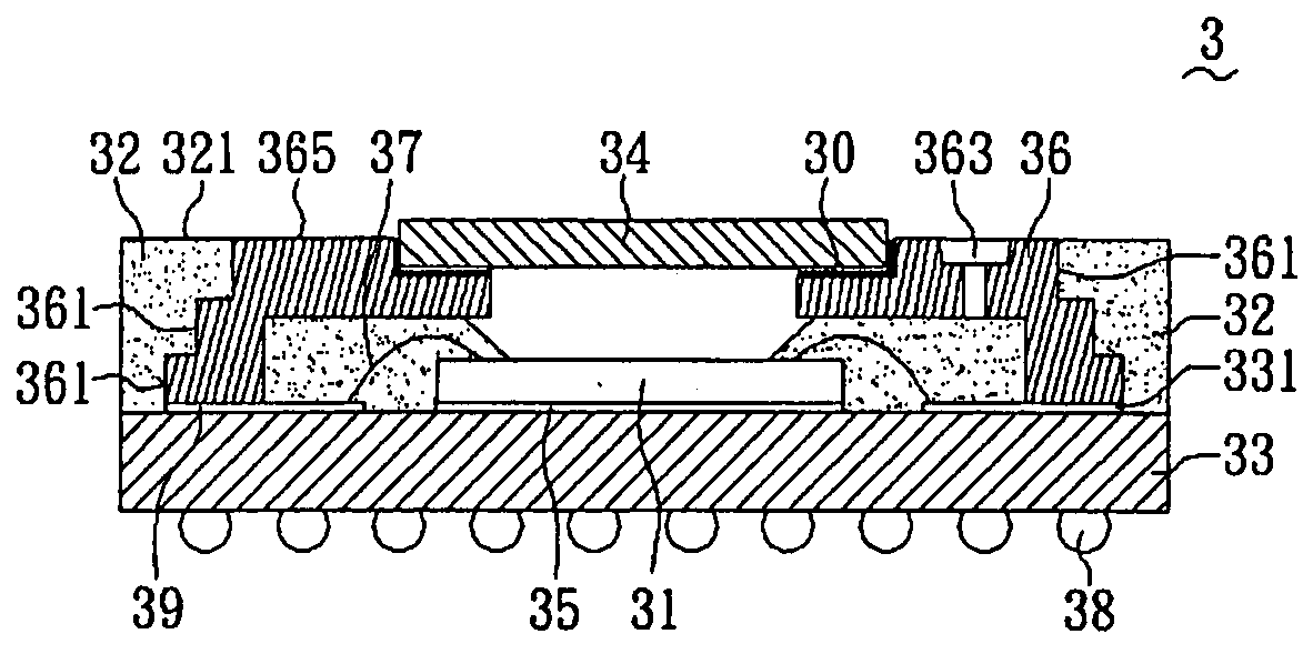
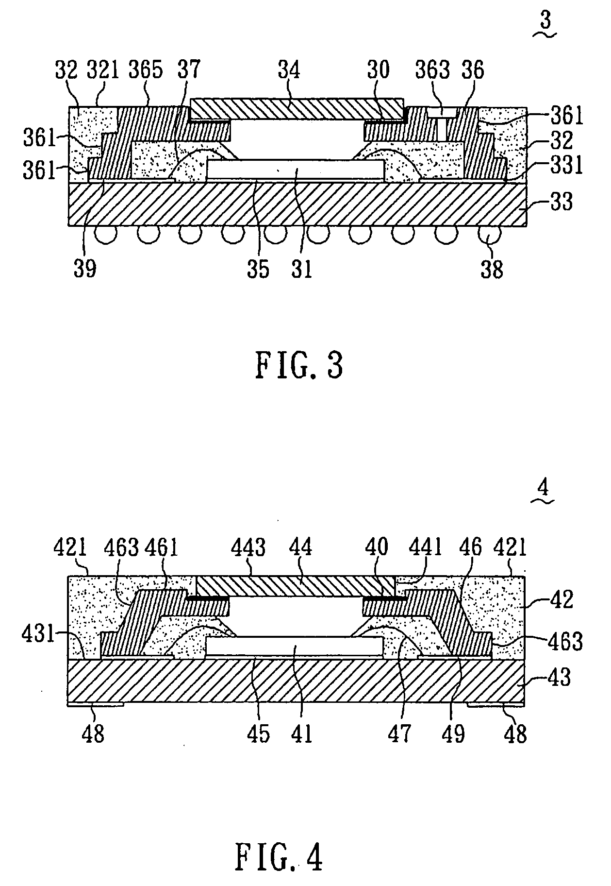
[0029]The process flow of making the image sensor package of the present invention is disclosed in FIG. 7. As shown, in step 700, the wafer having a plurality of image sensor chips is inspected. In step 702, the wafer is sawed to obtain multiple discrete image sensor chips (dies). In step 704, each die is bonded to the substrate by the adhesive. In step 706, curing is performed to cure the adhesive. In step 708, wire bonding is performed. In step 710, post bonding inspection is done. In step 712, the optical glass or IR filter is attached to the sensor housing by the adhesive. In step 714, curing is performed to cure the adhesive. In step 716, the sensor housing together with the optical glass (or IR filter) is mounted to the substrate by the adhesive. In step 718, curing is performed. In step 720 (optional), the gas-exit (optional) is sealed by the sealing material. In step 722, the gas-exit sealant curing is performed. In step 724, dispensing of encapsulation material is performed...
PUM
 Abstract
Description
Claims
Application Information