Transformer and transformer assembly

a transformer and transformer technology, applied in the field of transformers, can solve the problems of difficult reducing the size of this electronic product, unable to manufacture smaller components, etc., and achieve the effects of enhancing the fastening strength, reducing the thickness of an electronic product, and high fastening strength

Inactive Publication Date: 2009-02-19
ACBEL POLYTECH INC
View PDF11 Cites 10 Cited by
  • Summary
  • Abstract
  • Description
  • Claims
  • Application Information

AI Technical Summary

Benefits of technology

[0014]When the transformer is mounted on a circuit board to form a transformer assembly, the circuit board has a through hole corresponding to the position for where the transformer is going to be mounted. When the transformer is upwardly moved into the through hole of the circuit board, the connecting pins are able to be soldered on the solder pads on the back of the circuit board with their soldering surfaces. Because the transformer is mounted through and soldered on the circuit board, the total thickness of this transformer assembly will not include the thickness of the circuit board. Therefore it will help to reduce the thickness of an electronic product having this transformer assembly.
[0015]Another objective of the invention is to provide a transformer that has high fastening strength when being mounted on a circuit board. The approach is to form at least one fastener at another side of the lower flange opposite to the connecting pins. When the transformer being mounted on the circuit board, the at least one fastener can attach to the circuit board to enhance the fastening strength between the transformer and the circuit board.

Problems solved by technology

However some elements are unable to be manufactured into smaller ones.
It is noted that the thickness of an electronic product having this transformer assembly will include the thickness of the transformer (50) and the circuit board (60), and reducing the size of this electronic product is difficult.
When either of the forgoing transformers is mounted on the circuit board, the entire thickness of the transformer assembly will inevitably include the thickness of the circuit board.

Method used


Image

  • Transformer and transformer assembly
  • Transformer and transformer assembly
  • Transformer and transformer assembly

Examples


first embodiment

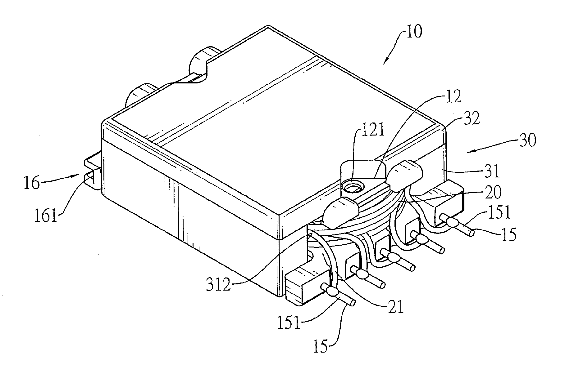
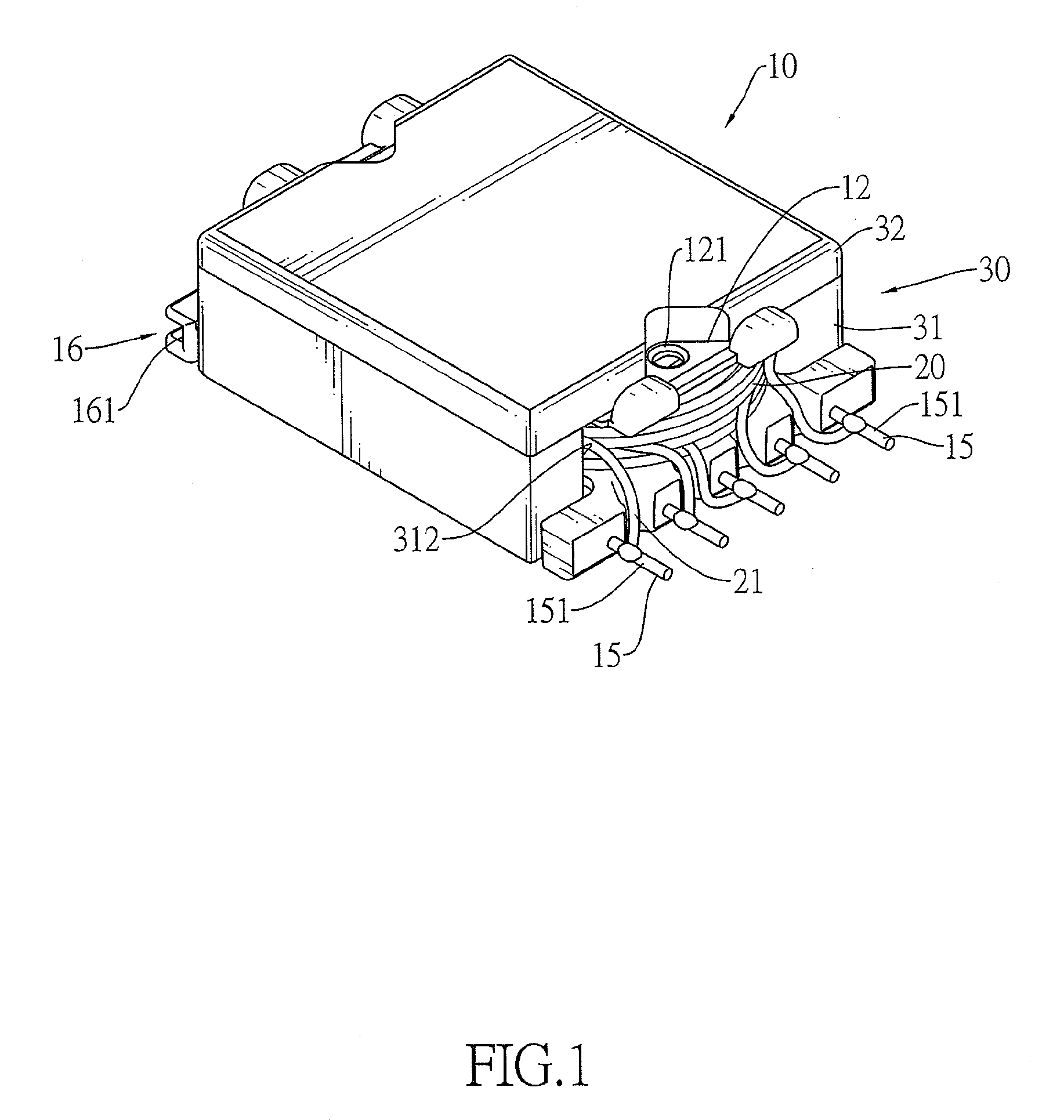
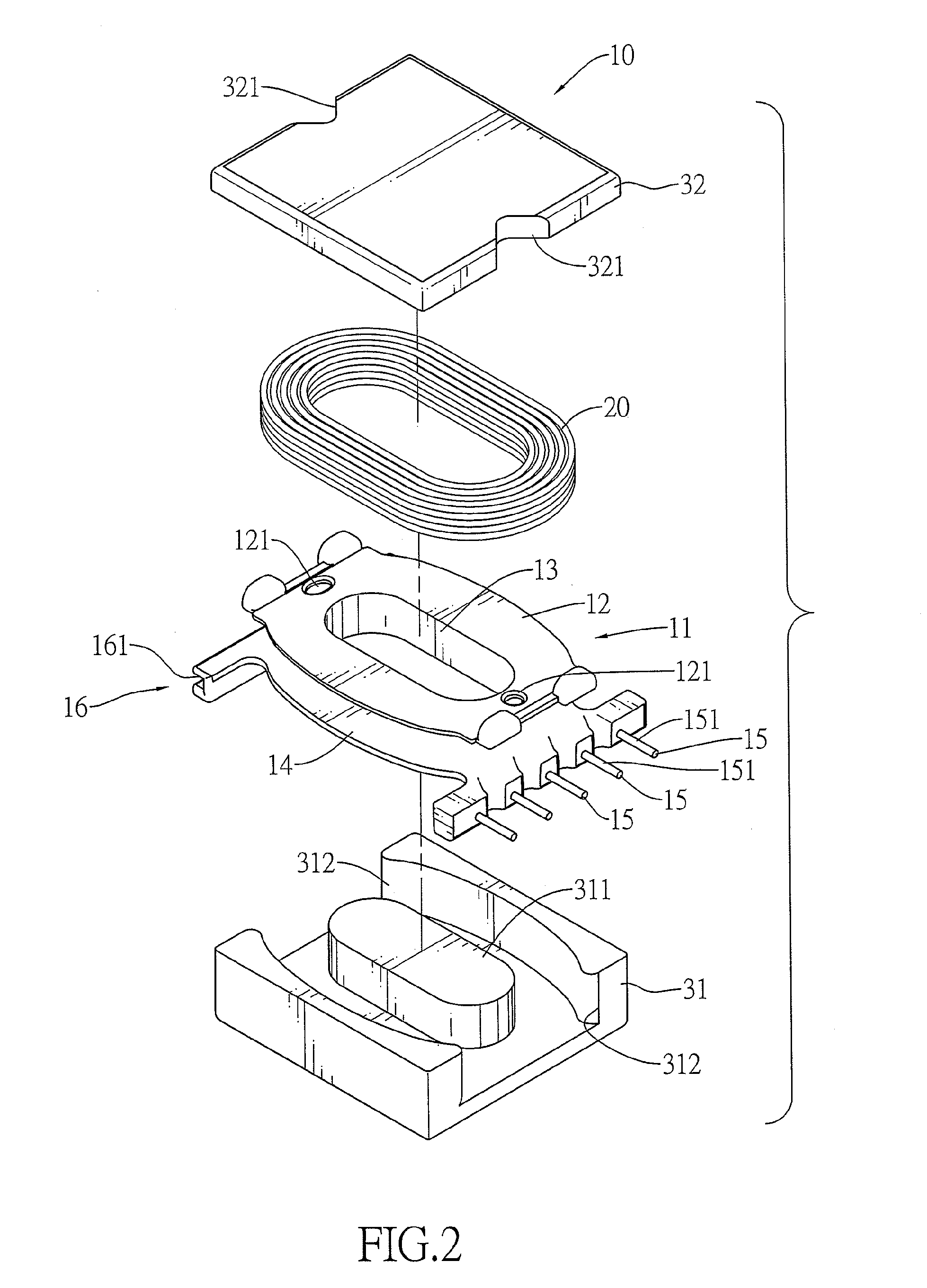
[0028]With reference to FIGS. 1 and 2, the transformer (10) in accordance with the present invention comprises a bobbin (11), a coil assembly (20) and a magnetic core assembly (30).

[0029]The bobbin (11) comprises a hollow winding core (13), an upper flange (12) and a lower flange (14). The hollow winding core (13) is flat-shaped and has an inner upper edge and an inner lower edge. The upper flange (12) is formed on and protrudes transversely from the inner upper edge of the hollow winding core (13), and has a top surface with at least one lead hole (121). In this embodiment, two lead holes (121) are formed through the upper flange (12) and are opposite to each other. The lower flange (14) is formed on and protrudes transversely from the inner lower edge of the hollow winding core (13) and has a bottom surface. Multiple connecting pins (15) transversely protrude from at least one side of the lower flange (14). Each connecting pin (15) has a top surface as a soldering surface (151).

[0...

third embodiment

[0035]With further reference with FIG. 6, the transformer (10b) has multiple fasteners being implemented as rivets (18) that can be respectively inserted into the fastener holes (42) and steadily abut against the upper surface of the circuit board (40).

[0036]With further references to FIGS. 3, 5, and 6, when mounting the transformer (10, 10a, 10b) on the circuit board (40), the transformer (10, 10a, 10b) is upwardly moved into the through hole (41) of the circuit board (40) until the soldering surfaces (151) of the connecting pins (15) respectively touch the solder pads on the back of the circuit board (40). The connecting pins (15) are then respectively and electrically soldered on the solder pads. Taking the first embodiment as an example, the transformer (10) has the engaging element (16) with the slot (161). When mounting the transformer (10) to the circuit board (40), the transformer (10) inclines with an angle in order to easily pass through the through hole (41) of the circui...


PUM

PropertyMeasurementUnit
thicknessaaaaaaaaaa
electrical energyaaaaaaaaaa
voltageaaaaaaaaaa

Abstract

The transformer has a bobbin, a coil assembly and a magnetic core assembly. The bobbin is mounted in the magnetic core assembly and has multiple connecting pins being formed on at least one side of a bottom surface of the bobbin. Each connecting pin has a top surface as a soldering surface that corresponds to a solder pad on a back of a circuit board. At least one fastener is further formed on the bottom surface of the circuit board. Therefore, when the transformer is mounted through the circuit board, the connecting pins are soldered on the back of the circuit board to reduce the total thickness of the combination of the transformer and the circuit board.

Description

BACKGROUND OF THE INVENTION[0001]1. Field of the Invention[0002]The present invention relates to a transformer and more particularly to a transformer that can be mounted to a circuit board to form a combination of the transformer and the circuit board with a thin thickness.[0003]2. Description of the Related Art[0004]Nowadays, electronic products have become much thinner and smaller, so the electronic elements for those electronic products have to be manufactured as small as possible. To satisfy the technical requirements, some integrated-circuit elements like transistors can be minimized by advanced semiconductor technologies. Passive circuit elements like resistors and capacitors can be made into smaller ones through advanced packaging technology or using some thinned substrate. However some elements are unable to be manufactured into smaller ones.[0005]Taking a transformer as an example, the transformer converts electrical energy, transfers electrical energy from one circuit to a...

Claims


Application Information

Patent Timeline
Patent Type & Authority Applications(United States)
IPC IPC(8): H01F27/06H01F27/00
CPCH01F5/04H01F27/29H01F27/325H01F2027/065H01F41/10H01F2005/043H01F30/06
Inventor YANG, CHAO-YUANCHANG, SHUN-TEYEH, CHANG-CHINGCHEN, JUI-CHIA
Owner ACBEL POLYTECH INC
Why Eureka
Try Eureka