

Display apparatus, driving method for display apparatus and electronic apparatus
a technology of display apparatus and driving method, which is applied in the direction of electric digital data processing, instruments, computing, etc., can solve the problems of image quality degradation of liquid crystal display apparatus, and achieve the effect of increasing power to the backlight and reducing the transmission factor
- Summary
- Abstract
- Description
- Claims
- Application Information
AI Technical Summary
Benefits of technology
Problems solved by technology
Method used
Image

Examples
first embodiment
[0108]FIGS. 2A to 2C show an example of a configuration of a liquid crystal display apparatus according to a first embodiment of the present invention and examples of a gate pulse waveform, respectively.
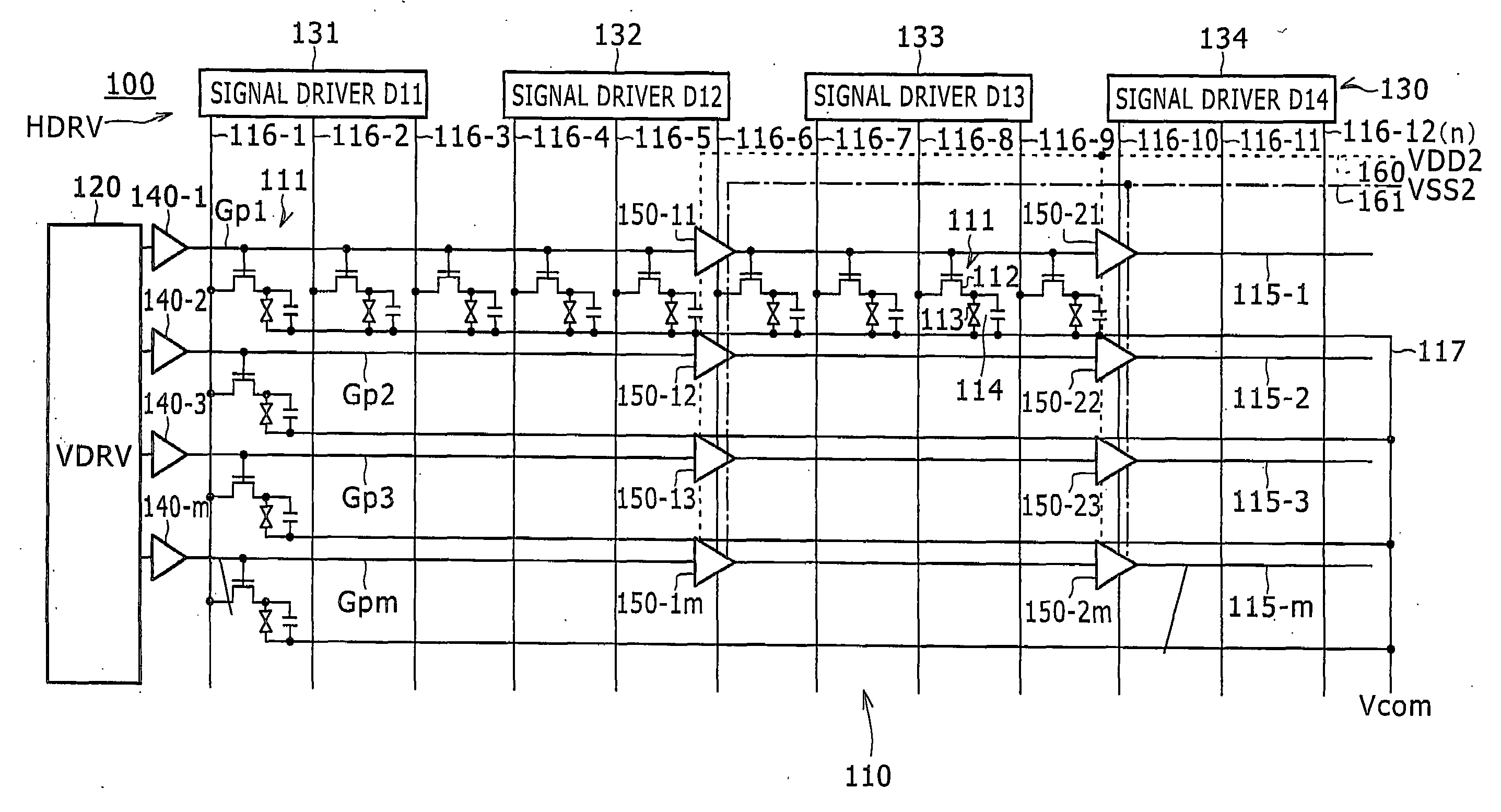
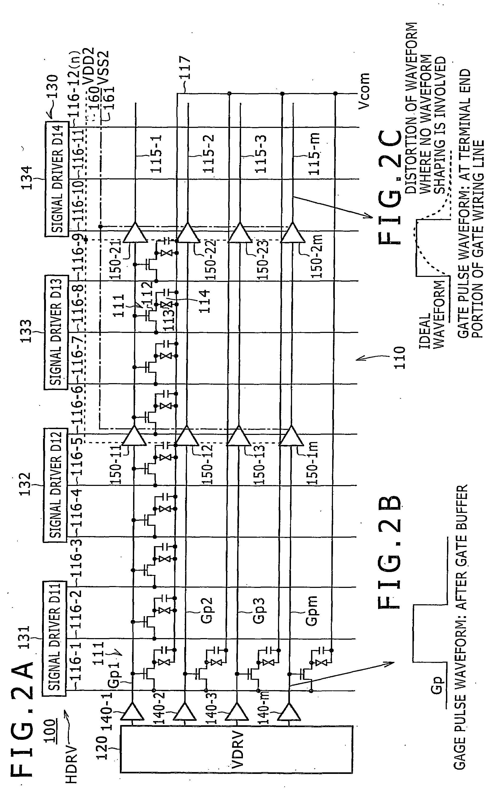
[0109]Referring first to FIG. 2A, the liquid crystal apparatus 100 includes an effective pixel region section 110, a vertical driving circuit (VDRV) 120 and a horizontal-driving circuit (HDRV) 130.
[0110]Gate buffers 140-1 to 140-m are disposed at the output stage of the vertical driving circuit 120 to gate lines 115-1 to 115-m which are scanning lines of a gate pulse GP.
[0111]In the liquid crystal apparatus 100 of the active matrix type of the present embodiment, waveform shaping circuits 150-11 to 150-1m and 150-21 to 150-2m for carrying out waveform shaping and voltage change for a gate pulse outputted from the vertical driving circuit 120 are disposed intermediately on the gate lines 115-1 to 115-m.
[0112]A gate pulse outputted from the vertical driving circuit 120 or the gate pul...
second embodiment
[0173]FIGS. 6A, 6B, and 6C show an example of a configuration of a liquid crystal display apparatus according to a second embodiment of the present invention and examples of a gate pulse waveform, respectively.
[0174]Referring first to FIG. 6A, the liquid crystal display apparatus 100A according to the present second embodiment is similar in configuration to but different in the arrangement position of the waveform shaping circuits 150 from the liquid crystal apparatus 100 according to the first embodiment described above.
[0175]In particular, in the liquid crystal apparatus 100 of the first embodiment described above, the supply lines 160 and 161 for the voltages VDD2 and VSS2 to be supplied to the waveform shaping circuits 150 and the waveform shaping circuits 150 are disposed on the same coordinates in the horizontal direction.
[0176]In contrast, in the liquid crystal display apparatus 100A of the present second embodiment, the supply lines 160 and 161 for the voltages VDD2 and VSS2...
third embodiment
[0182]FIGS. 7A, 7B, and 7C show an example of a configuration of a liquid crystal display apparatus according to a third embodiment of the present invention and examples of a gate pulse waveform, respectively.
[0183]Referring first to FIG. 7A, the liquid crystal display apparatus 100B according to the present third embodiment is similar in configuration to but different in the arrangement position of the waveform shaping circuits 150 from the liquid crystal display apparatus 100 and 100A according to the first and second embodiments described above.
[0184]In particular, in the liquid crystal display apparatus 100 and 100A according to the first and second embodiments, the supply lines 160 and 161 for the voltages VDD2 and VSS2 to be supplied to the waveform shaping circuits 150 and the waveform shaping circuits 150 are disposed at the same coordinates in the horizontal direction.
[0185]Or conversely, the supply lines 160 and 161 for the voltages VDD2 and VSS2 to be supplied to the wave...
PUM
 Abstract
Description
Claims
Application Information