

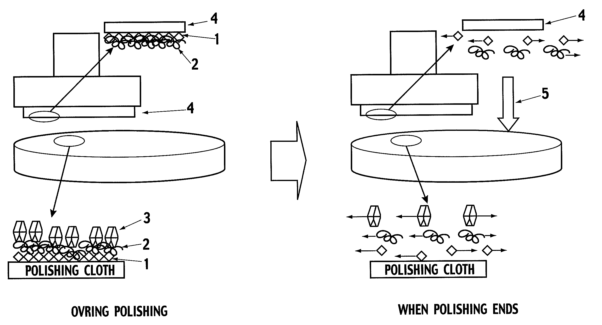
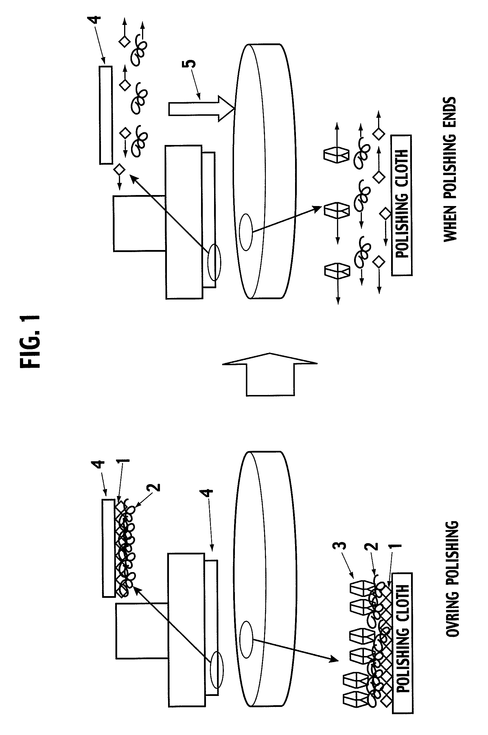
CMP Abrasive Slurry for Polishing Insulation Film, Polishing Method, and Semiconductor Electronic Part Polished by the Polishing Method
a technology of abrasive slurry and insulation film, which is applied in the direction of lapping machines, manufacturing tools, other chemical processes, etc., can solve the problems of not flattening the insulation film over the entire wafer surface, preventing easy process control, and not being able to completely remove the deposited particles, etc., to achieve high throughput and cost-effective polishing
- Summary
- Abstract
- Description
- Claims
- Application Information
AI Technical Summary
Benefits of technology
Problems solved by technology
Method used
Image

Examples
example 1
[0128]One kg of the cerium oxide particles prepared above, 23 g of an aqueous ammonium polyacrylate salt solution (weight-average molecular weight: 9000, 40 wt %-aqueous solution) and 8,977 g of deionized water were mixed, and the mixture was dispersed while agitated under ultrasonication for 10 minutes. The slurry obtained was filtered through a 1-micron filter, and deionized water was added to the filtrate, to give a cerium oxide slurry at a solid matter concentration of 5 wt %. The pH of the cerium oxide slurry was 8.3. The median value of the diameter of the slurry particles, as determined by diluting the slurry to a suitable concentration and measuring the diluted slurry by using a laser-scattering particle size distribution analyzer (Master Sizer Microplus, manufactured by Malvern) at a refractive index of 1.93, was 190 nm.
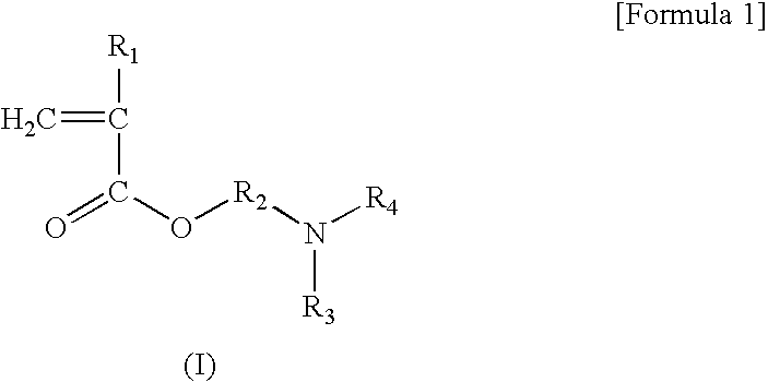
[0129]600 g of the cerium oxide slurry above (solid matter: 5 wt %), 3.6 g of the water-soluble polymer (I) solution obtained in Preparative Example 1 and 2...
example 2
[0136]An abrasive slurry (B) (solid matter: 1 wt %) was prepared in a similar manner to Example 1, except that the water-soluble polymer (I) solution was replaced with the water-soluble polymer (II) solution obtained in Preparative Example 2. The pH of the abrasive slurry (B) was 8.3. The median diameter of the particles in the abrasive slurry (B), as determined in a similar manner to Example 1, was 190 nm.
[0137]The insulation film layer was polished in a similar manner to Example 1, while the abrasive slurry (A) was replaced with the abrasive slurry (B), to give the results shown in Table 1.
example 3
[0138]An abrasive slurry (C) (solid matter: 1 wt %) was prepared in a similar manner to Example 1, except that the water-soluble polymer (I) solution was replaced with the water-soluble polymer (III) solution obtained in Preparative Example 3. The pH of the abrasive slurry (C) was 8.2. The median diameter of the particles in the abrasive slurry (C), as determined in a similar manner to Example 1, was 190 nm.
[0139]The insulation film layer was polished in a similar manner to Example 1, while the abrasive slurry (A) was replaced with the abrasive slurry (C), to give the results shown in Table 1.
PUM
| Property | Measurement | Unit |
|---|---|---|
| diameter | aaaaa | aaaaa |
| diameter | aaaaa | aaaaa |
| crystallite diameter | aaaaa | aaaaa |
Abstract
Description
Claims
Application Information