Micro actuator

Inactive Publication Date: 2009-02-26
SUNONWEALTH ELECTRIC MACHINE IND
11 Cites 7 Cited by

AI-Extracted Technical Summary

Problems solved by technology

For sake of large-area friction between the plate 10 and the substrate 12 of a conventional micro actuator, the abrasion therebetween is relati...

Benefits of technology

[0010]In view of the foregoing concern, the present invention thus provides a micro actuator capable of effectively reducing a contact area between a plate and a substrate thereof, in which the micro actuator is located on a substrate and includes a plate and a bushing.
[0011]A triangular shape or an arc-...

Abstract

The present invention relates to a micro actuator, which is located on a substrate and includes a plate and a bushing. A rear end of the plate exhibits a tapered triangular shape or an arc-like shape or has at least a bump disposed on a bottom surface of the rear end of the plate, making that a non-planar contact is present between the rear end of the plate and the substrate when both are contacted, so as to effectively reduce the friction and driving voltage and prolong the lifespan of components.

Application Domain

Contact surface shape/structureElectrostatic/electro-adhesion relays +3

Technology Topic

Micro actuatorVoltage +2

Image

  • Micro actuator
  • Micro actuator
  • Micro actuator

Examples

  • Experimental program(1)

Example

[0016]To make the object, features and efficacy of the present invention more comprehensive, preferred embodiments of the present invention are enumerated along with the detailed illustrative description.
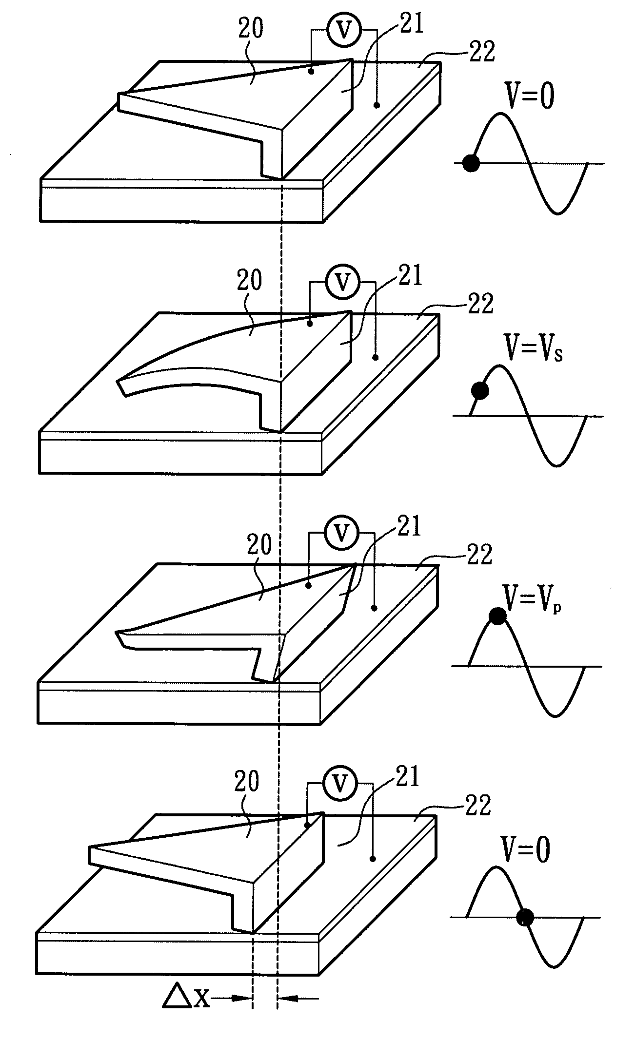
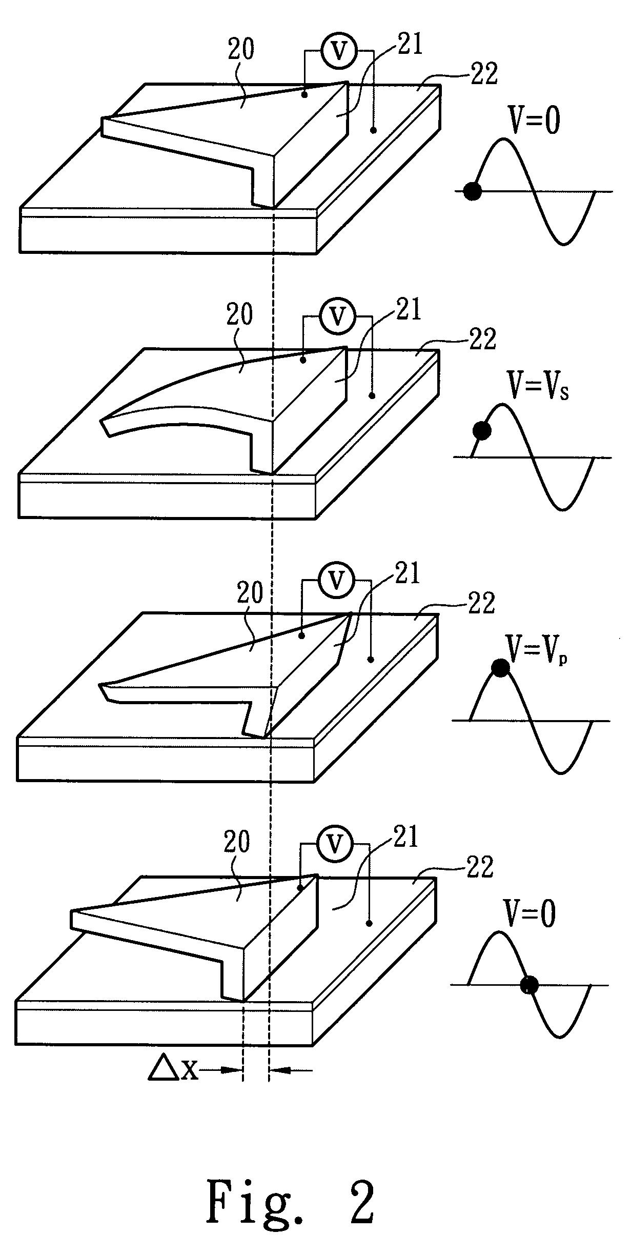
[0017]Please refer to FIG. 2. A micro actuator is located on a substrate 22 and includes a plate 20 and a bushing 21, wherein the plate 20 has a tapered triangular shape formed at a rear end of the plate 20.
[0018]When a positive bias voltage is applied externally, the plate 20 is attracted by the substrate 22 due to electrostatic force, so that an end point is contacted with the substrate 22. Meanwhile, as the friction, due to the contact of the plate 20 with the substrate 22, is less than the friction between the bushing 21 and the substrate 22, a significant small area of the rear end of the plate 20 is in contact with the substrate 22, further causing that the bushing 21 is extruded and shrunken and possesses an elastic tension.
[0019]As the plate 20 only has a non-planar contact with the substrate 22 and the plate 20 bends upwardly to alleviate the friction between the bushing 21 and the substrate 22 when it bounces back, adding that the rear end of the plate 20 of the micro actuator in the present invention forms a tapered triangular shape, a point contact is present between the rear end of the plate 20 and the substrate 22 when both are contacted, so as to effectively reduce the friction and driving voltage and prolong the lifespan of components.
[0020]Please further refer to FIG. 3, which is a second preferred embodiment of the present invention. An arc-like shape is formed at the rear end of the plate 20. Therefore, when the rear end of the plate 20 is contacted with the substrate 22, likewise, a point contact is present therebetween, so as to effectively reduce the friction and driving voltage and prolong the lifespan of components.
[0021]Please refer to FIG. 4, which is the third preferred embodiment of the present invention. The micro actuator is located on a substrate 22 and includes a plate 20 and a bushing 21, and a bottom surface of a rear end of the plate 20 has at least a bump 23.
[0022]By means of the design of the bump 23, when the rear end of the plate 20 is contacted with the substrate 22, a point contact is present therebetween, so as to reduce the friction and driving voltage and prolong the lifespan of components.
[0023]In sum, the present invention possesses the aforementioned advantages indeed. From the above-mentioned characteristics those features not only have a novelty among similar products and a progressiveness but also have an industry utility.
[0024]While the invention has been described in terms of what is presently considered to be the most practical and preferred embodiments, it is to be understood that the invention needs not be limited to the disclosed embodiments. On the contrary, it is intended to cover various modifications and similar arrangements included within the spirit and scope of the appended claims, which are to be accorded with the broadest interpretation so as to encompass all such modifications and similar structures.

PUM

no PUM

Description & Claims & Application Information

We can also present the details of the Description, Claims and Application information to help users get a comprehensive understanding of the technical details of the patent, such as background art, summary of invention, brief description of drawings, description of embodiments, and other original content. On the other hand, users can also determine the specific scope of protection of the technology through the list of claims; as well as understand the changes in the life cycle of the technology with the presentation of the patent timeline. Login to view more.

Similar technology patents

Longitudinal wave type tabletting and crushing machine for powder coatings

ActiveCN105642393AReduce contact areaAvoid large area adhesion
Owner:济宁高新科达科技项目服务有限公司

Moulding technology for lead-boron polyethylene sheet

InactiveCN1504321AReduce contact areaReduce lead vapor pollution
Owner:NUCLEAR POWER INSTITUTE OF CHINA

Epoxy resin system, preparation method thereof and prepreg

Owner:AEROSPACE RES INST OF MATERIAL & PROCESSING TECH +1

Classification and recommendation of technical efficacy words

  • reduce contact area

Wafer-Supporting Device and Method for Producing Same

ActiveUS20130014896A1improve uniformity of film thickness and film propertyreduce contact area
Owner:ASM JAPAN

Semiconductor device and method for fabricating the same

InactiveUS20070096212A1interconnection resistance increasereduce contact area
Owner:PANASONIC CORP

Tidal-flat ship

Owner:陈兆红

Multi-substrate combining detection method based on laser measurement

ActiveCN103292748Agive way directlyReduce contact area
Owner:XIAN AIRCRAFT DESIGN INST OF AVIATION IND OF CHINA
Why Eureka
Try Eureka