
Multilayer electronic component and method for manufacturing the same

a technology of electronic components and components, applied in the direction of fixed capacitor details, coatings, capacitors, etc., can solve the problems of large stress generated by substrate warping, deformation of multi-layer electronic components, crack generation, etc., to suppress the deterioration of electrical properties and crack generation, improve the effect of reducing stress, and reduce the effect of generating cracks

Inactive Publication Date: 2009-02-26
MURATA MFG CO LTD
View PDF24 Cites 52 Cited by
  • Summary
  • Abstract
  • Description
  • Claims
  • Application Information

AI Technical Summary

Benefits of technology

[0014]To overcome the problems described above, preferred embodiments of the present invention provide a multilayer electronic component and a method for manufacturing the same, the multilayer electronic component having an improved effect of reducing a stress caused by substrate warping, suppressing the deterioration of the electrical properties and the generation of cracks, and having a high effective volume ratio.
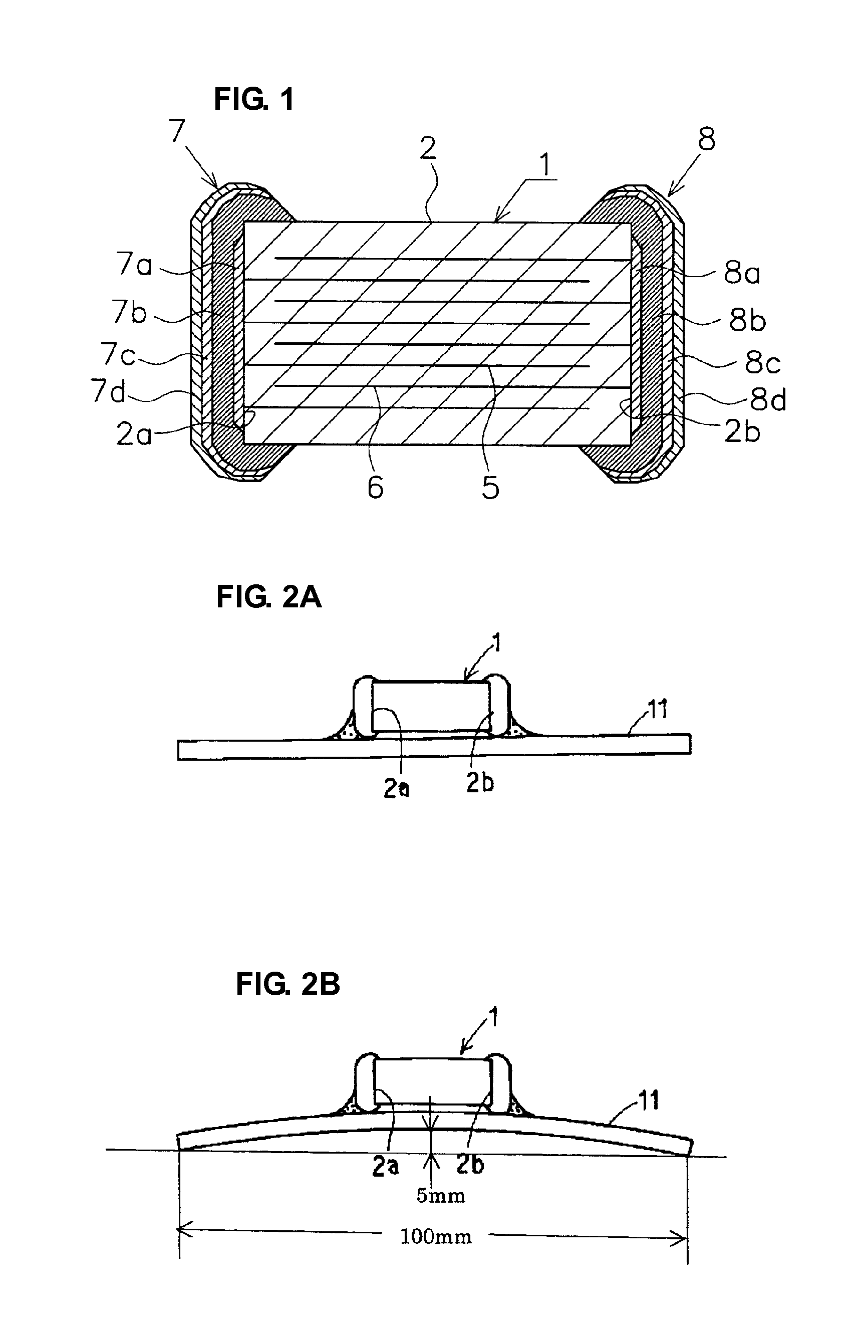
[0022]Since the first electrode layers formed by plating, and preferably electroplating, are provided as underlayers for the second electrode layers made of a conductive resin, an effect of reducing stress generated by substrate warping is significantly improved, and deteriorations in the electrical properties and defects, such as cracks, can be reliably suppressed.
[0023]In addition, since the first electrode layers are formed by plating, the thickness of each of the terminal electrodes can be decreased, and the effective volume ratio of the multilayer electronic component can be improved.
[0024]Furthermore, since the first electrode layers are directly formed on the exposed surfaces of the internal electrodes by plating, a dipping step or a firing step is not required, and the manufacturing process can be simplified, accordingly.

Problems solved by technology

As a result, the electrical properties of the multilayer electronic component may be degraded and cracks may be generated in the multilayer electronic component.
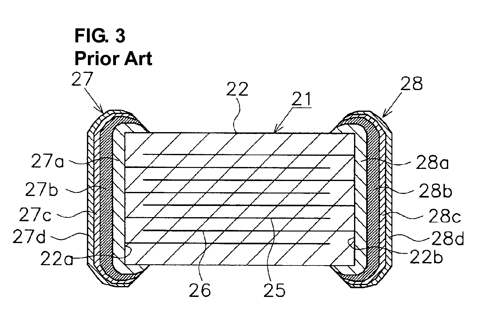
Thus, in the multilayer ceramic capacitor disclosed in Japanese Unexamined Patent Application Publication No. 5-144665, a large stress generated by the substrate warping cannot be sufficiently reduced.
In particular, a stress is likely to be concentrated in a curved portion of the terminal electrode, and as a result, cracking is likely to occur in this portion.
As a result, there is a problem in that an effective volume ratio of the multilayer ceramic capacitor is decreased.

Method used


Image

  • Multilayer electronic component and method for manufacturing the same
  • Multilayer electronic component and method for manufacturing the same
  • Multilayer electronic component and method for manufacturing the same

Examples


example 1

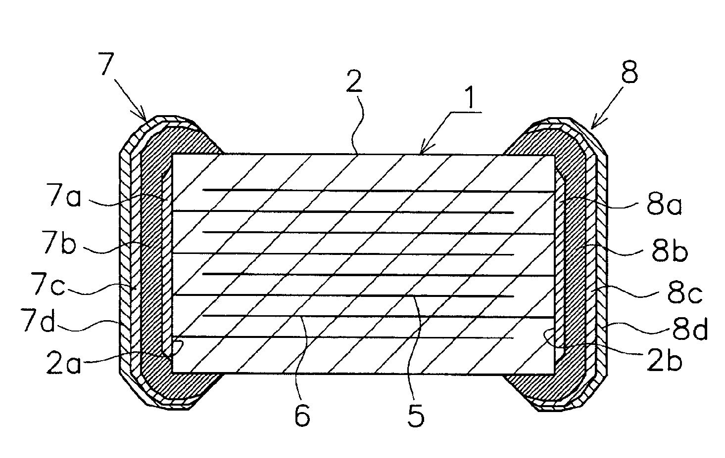
[0051]As shown in FIG. 1, a multilayer ceramic base body was prepared and which had an approximately rectangular parallelepiped shape of about 3.2 mm long, about 1.6 mm wide, and about 1.6 mm thick. The base body was made of a titanium barium-based dielectric ceramic, and internal electrodes were made of Ni. In addition, the thickness of one dielectric layer between adjacent internal electrodes was about 4.4 μm, the number of lamination layers provided for the desired electrostatic capacitance was about 263, and the internal electrodes were alternately exposed at two opposed end surfaces. In addition, at this stage, withdrawal lengths d of the internal electrodes with respect to the surfaces 2a and 2b at which the internal electrodes were exposed were a maximum of about 10 μm.

[0052]Sand blasting was performed on the multilayer ceramic base body, and the withdrawal lengths d of the internal electrodes with respect to the surfaces at which the internal electrodes were exposed were set...


PUM

PropertyMeasurementUnit
lengthaaaaaaaaaa
lengthaaaaaaaaaa
temperatureaaaaaaaaaa

Abstract

A multilayer electronic component includes a base body, internal electrodes disposed inside the base body and extending to exterior surfaces thereof, and terminal electrodes provided on the exterior surfaces of the base body and connected to the internal electrodes. The terminal electrodes include first electrode layers defined by plating layers, and preferably electroplating layer, and second electrode layers made of a conductive resin and provided on the first electrode layers.

Description

BACKGROUND OF THE INVENTION[0001]1. Field of the Invention[0002]The present invention relates to a multilayer electronic component and a method for manufacturing the same, and more particularly, to a method for forming terminal electrodes of a multilayer electronic component.[0003]2. Description of the Related Art[0004]Conventionally, a multilayer electronic component defined by a multilayer ceramic capacitor includes a base body made of a dielectric substance, internal electrodes provided therein, and terminal electrodes connecting the internal electrodes.[0005]This multilayer electronic component is often surface-mounted on a substrate, such as a circuit substrate. In this case, the terminal electrodes and the substrate are bonded and fixed to each other by soldering. However, when the substrate is warped, a stress is applied to the multilayer electronic component mounted thereon. As a result, the electrical properties of the multilayer electronic component may be degraded and cra...

Claims


Application Information

Patent Timeline
Patent Type & Authority Applications(United States)
IPC IPC(8): H01G4/228B05D5/12C25D5/02
CPCH01G4/30H01G4/2325
Inventor MOTOKI, AKIHIROOGAWA, MAKOTOUKUMA, YUJI
Owner MURATA MFG CO LTD
Learn More