

Electronic device and method of forming same
a technology of electronic devices and forming methods, applied in the direction of duplex signal operation, electrical apparatus construction details, electrical apparatus casings/cabinets/drawers, etc., can solve the problems of further limited extent to which the size of the extent to which such devices may be reduced
- Summary
- Abstract
- Description
- Claims
- Application Information
AI Technical Summary
Benefits of technology
Problems solved by technology
Method used
Image

Examples
Embodiment Construction
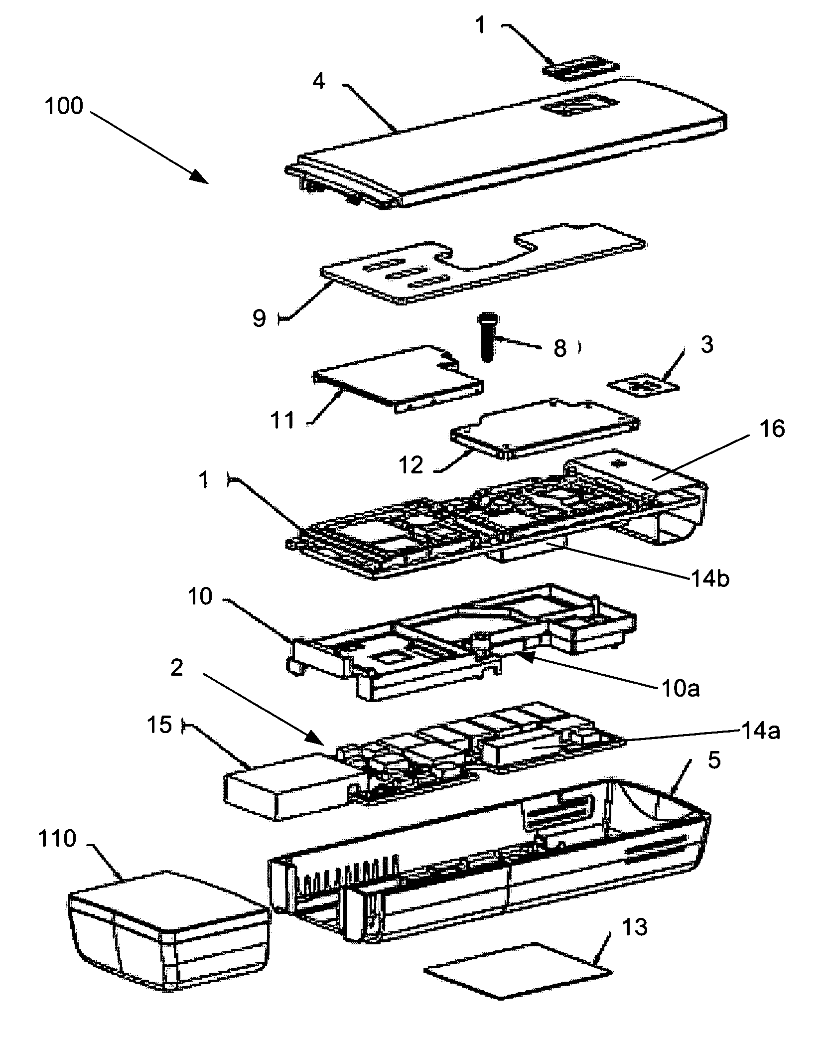
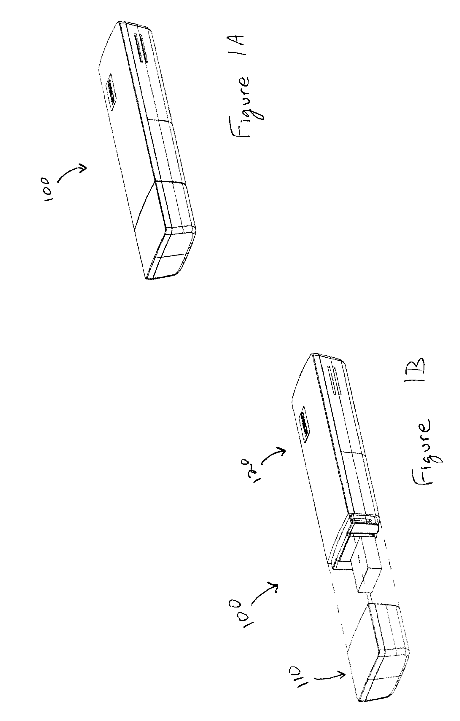
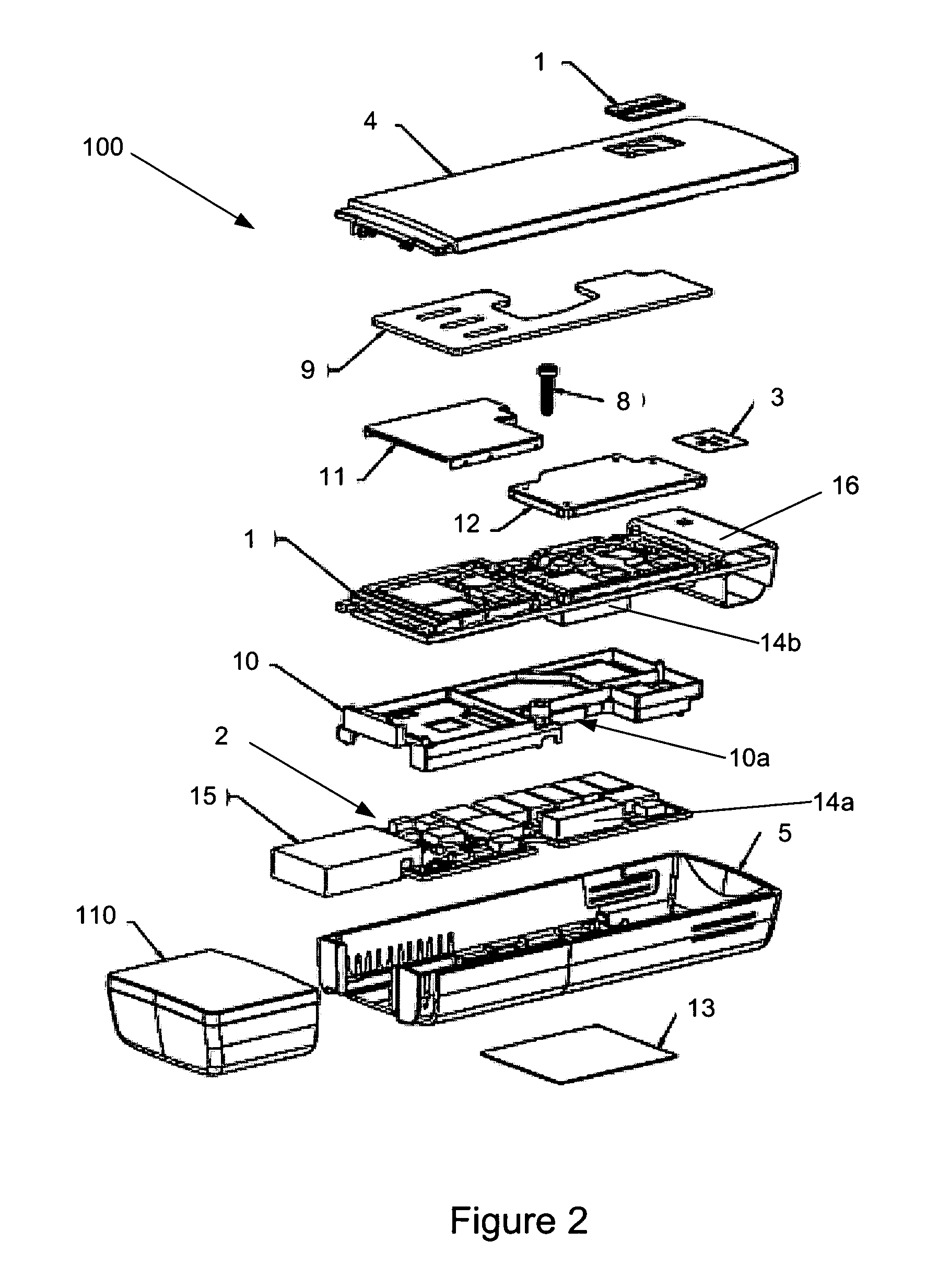
[0026]Referring to FIGS. 1A and 1B, an electronic device according to an embodiment of the present invention is illustrated. The electronic device 100 may be any type of electronic device with electronic components therein. In the illustrated embodiment, the electronic device 100 is a modem device adapted to provide wireless communication.
[0027]The electronic device 100 includes a main body 120 and a cap 110. FIG. 1A illustrates the electronic device 100 in the closed position with the cap covering an end of the main body, while FIG. 1B illustrates the electronic device 100 in an open position with an end of the main body 120 exposed. The main body 120 includes various electronic components (described below), as well as a connector for coupling the electronic device 100 with another device, such as a communication device. The communication device may be, for example, a desktop computer, a laptop computer, a portable phone, a personal digital assistant (PDA) or the like.
[0028]Referri...
PUM
| Property | Measurement | Unit |
|---|---|---|
| electromagnetic | aaaaa | aaaaa |
| transfer of heat | aaaaa | aaaaa |
| structural rigidity | aaaaa | aaaaa |
Abstract
Description
Claims
Application Information