Semiconductor integrated circuit

a technology of integrated circuits and semiconductors, applied in the field of semiconductor integrated circuits, can solve the problems of inefficiency in calibrating absolute variations in characteristics, and achieve the effect of efficiently calibrating characteristics and efficiently calibrating characteristics

Active Publication Date: 2009-02-26
RENESAS ELECTRONICS CORP
View PDF4 Cites 30 Cited by
  • Summary
  • Abstract
  • Description
  • Claims
  • Application Information

AI Technical Summary

Benefits of technology

[0034]Advantageous effects obtained by representative ones of various inventions disclosed in the present application will be described in brief as follows:
[0035]There can be provided an RF analog LSI capable of efficiently calibrating characteristics of a pair of reception low-pass filters th

Problems solved by technology

Thus, the present inventors et al. have reached a conclusion that it is not efficient to calibrate the absolute

Method used


Image

  • Semiconductor integrated circuit
  • Semiconductor integrated circuit
  • Semiconductor integrated circuit

Examples


embodiment

Description of Embodiment

[0099]Preferred embodiments will next be described in further detail.

>

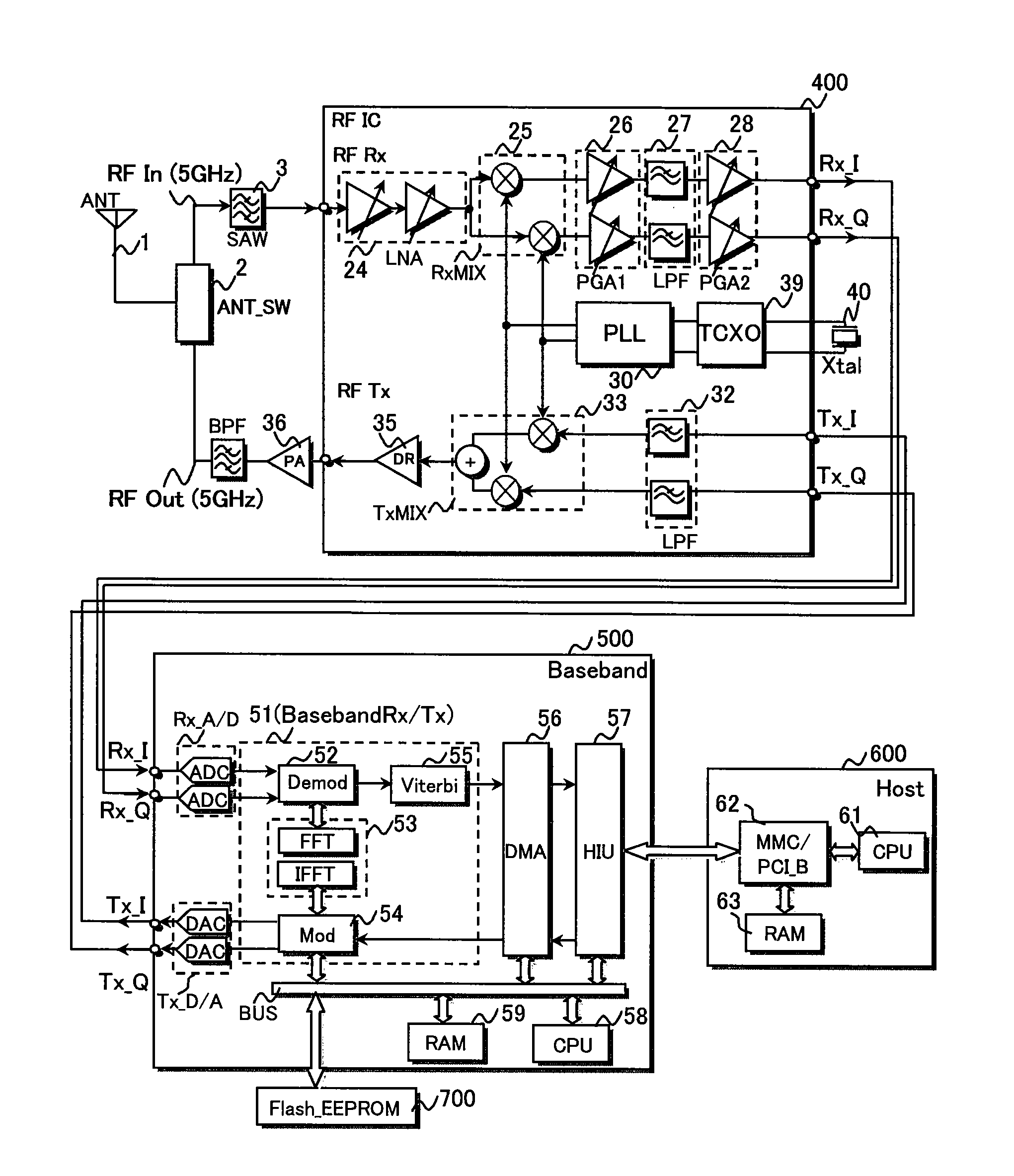
[0100]FIG. 1 is a diagram showing a wireless LAN system including a semiconductor integrated circuit corresponding to an RF analog circuit 400 and a baseband processing LSI 500 according to one embodiment of the present invention. The wireless LAN system shown in FIG. 1 can be commonly used in LAN equipment of a wireless LAN and an access point of a communication partner.

[0101]An antenna switch 2 is coupled to an antenna 1, and the supply of an RF reception input signal from the antenna 1 to a receiver system and the supply of an RF transmission output signal from a transmitter system to the antenna 1 are performed by time division multiple access (TDMA). The wireless LAN system shown in FIG. 1 enables communications at a maximum throughput of 100 Mbps based on the IEEE802.11n standard.

>

>

[0102]Since a direct downconversion receiver system RF Rx of the RF analog semiconductor integrated cir...


PUM


Abstract

The present invention aims to efficiently calibrate the characteristics of a pair of reception or transmission low-pass filters by a receiving or transmitting circuit. A semiconductor integrated circuit includes an RF receiver that processes an RF reception signal, an RF transmitter that generates an RF transmission signal and a frequency synthesizer. A reception low-pass filter of the RF receiver suppresses undesired components contained in I and Q baseband reception signals. A transmission low-pass filter of the RF transmitter suppresses noise due to D/A conversion, which is contained in I and Q transmission analog baseband signals. A calibration test signal is supplied to the inputs of the pair of reception or transmission low-pass filters. A difference in phase between the pair of filters is detected by a phase detection unit. A calibration controller calibrates a relative mismatch between the cut-off frequencies of the pair of filters.

Description

CLAIM OF PRIORITY[0001]The present application claims priority from Japanese patent application JP 2007-213564 filed on Aug. 20, 2007, the content of which is hereby incorporated by reference into this application.FIELD OF THE INVENTION[0002]The present invention relates to a semiconductor integrated circuit equipped with an RF transceiver, and particularly to a technique useful to efficiently calibrate a pair of built-in low-pass filters for quadrature signals by the RF transceiver.BACKGROUND OF THE INVENTION[0003]As compared with the wireless LAN system of the current IEEE802.11b / g, IEEE802.11a provides a data rate of about 5 times the current data rate, at least an overall system capacity of 20 times the current capacity as the standard for a novel wireless LAN based on the Orthogonal Frequency Division Multiplex (OFDM) for a demand for wide wireless communication. In a 5 GHz frequency band, a wireless LAN is shifted from 2.4 GHz to 5 GHz with the advantage of a high data rate. I...

Claims


Application Information

Patent Timeline
IPC IPC(8): H04B1/38H04B1/26H04B1/3822H04B1/40H04L27/00H04L27/18
CPCH04B1/30
Inventor KAWABE, MANABUTANAKA, SATOSHINARA, YOSHIKAZU
Owner RENESAS ELECTRONICS CORP
Why Eureka
Try Eureka