E-beam inspection structure for leakage analysis

a leakage analysis and inspection structure technology, applied in the direction of electrical equipment, electronic circuit testing, instruments, etc., to achieve the effect of reducing repetition

Inactive Publication Date: 2009-03-05
CHARTERED SEMICONDUCTOR MANUFACTURING
View PDF8 Cites 101 Cited by
  • Summary
  • Abstract
  • Description
  • Claims
  • Application Information

AI Technical Summary

Problems solved by technology

For instance, some of these advantages may be mutually contradictory, in that they cannot be simultaneously present in a single embodiment.

Method used


Image

  • E-beam inspection structure for leakage analysis
  • E-beam inspection structure for leakage analysis
  • E-beam inspection structure for leakage analysis

Examples


example 1

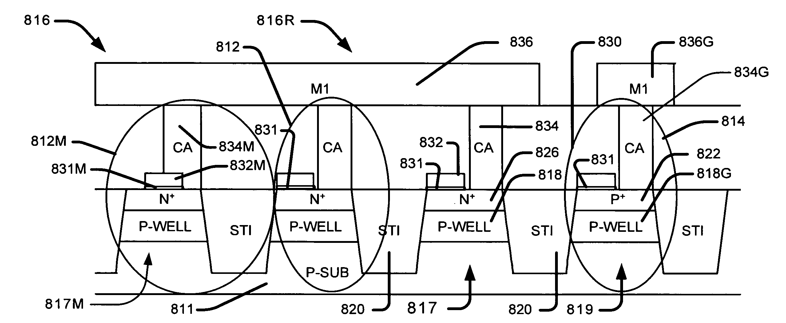
[0186]Test Structure #1 (116)—High count of BVC

[0187]Test Structure #2 (216)—Low count of BVC

[0188]leakage must be due to Si defect, as test structure #2 (216) (sensitive for STI 220 leakage) has a low count of BVC.

example 2

[0189]Test Structure #1 (116)—Low count of BVC

[0190]Test Structure #2 (216)—High count of BVC

[0191]leakage could be from STI as test structure #2 (216) is more sensitive to STI 220 leakage and test structure #1 (116) is more sensitive to Si leakage.

[0192]If both test structures #1 (116) and #2 (216) have high counts of BVC it is reasonable to suspect we have both Si and STI leakage issues. However we can draw better conclusions by looking at the rest of the test structures #3 (316) . . . #8 (816) and isolate each of the regions, if any, that have potential problem.

Non-Limiting Exemplary Embodiments

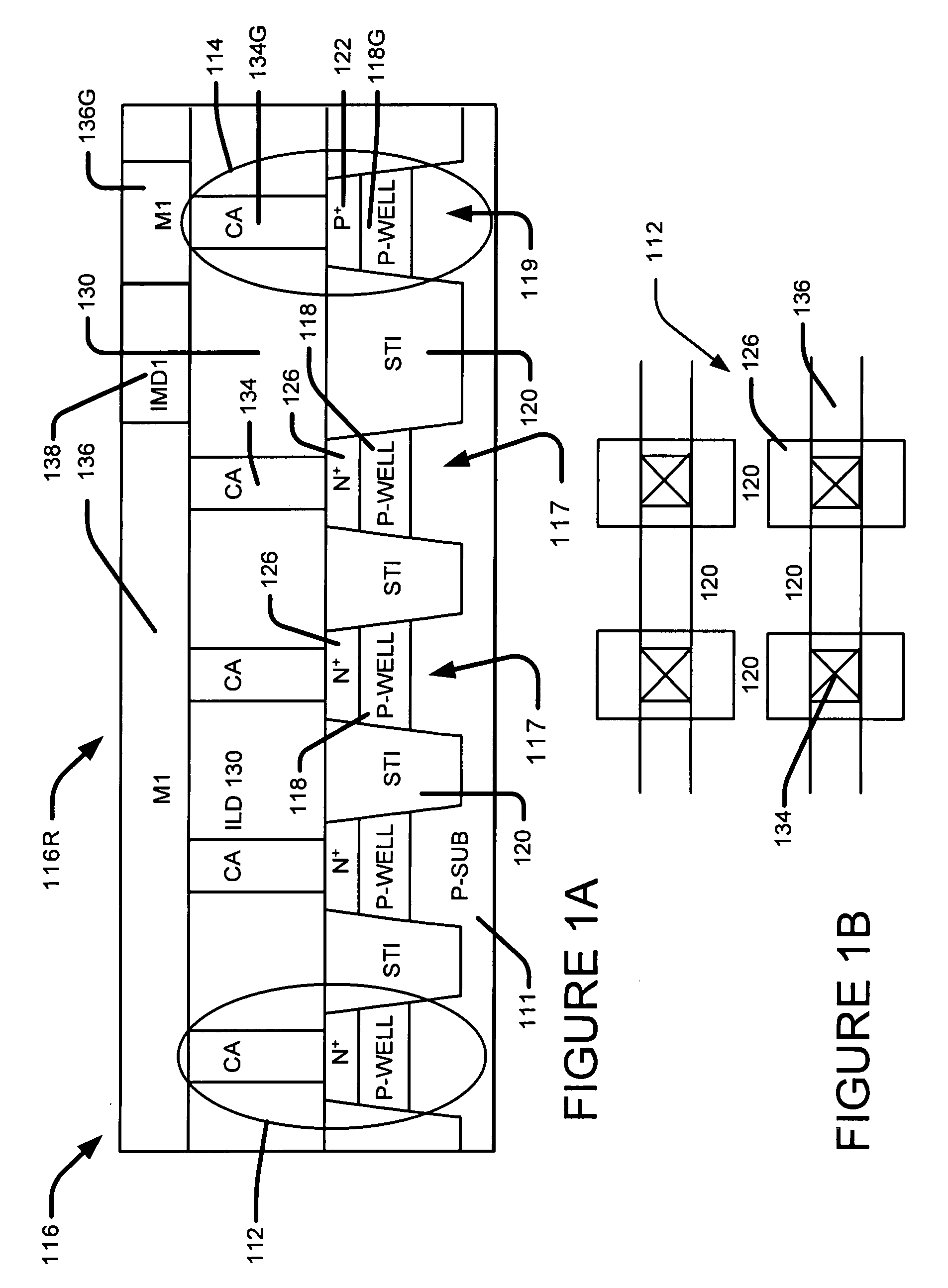
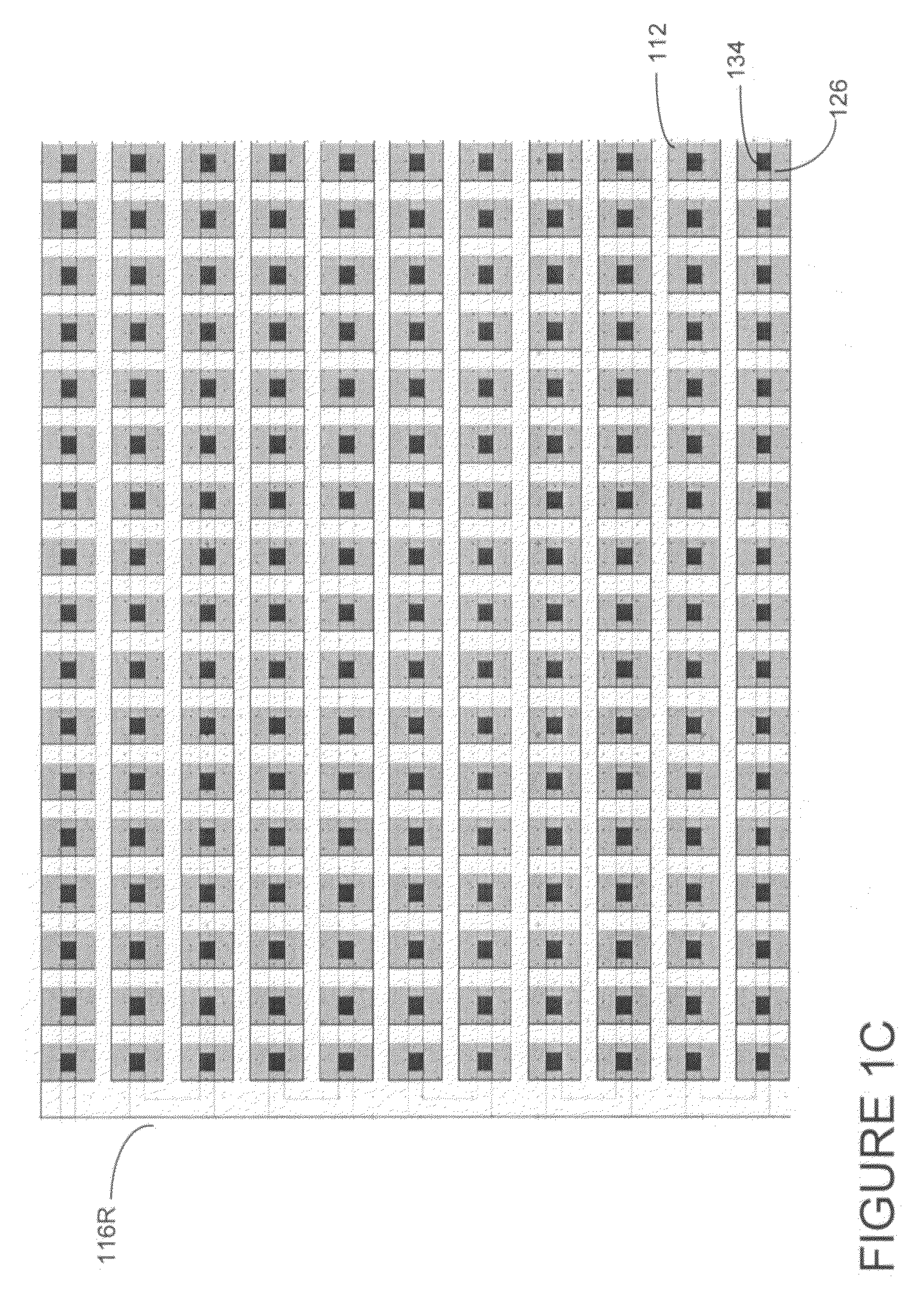
[0193]The exemplary embodiment test structures 116, 216, 316 . . . 816, for example, can be used on a product wafer or on a monitor wafer. The test structures 116, 216, 316 . . . 816 may be formed in the kerf area between chips on a wafer, for example.

[0194]It is noted that 1 or more, 2 or more, 3 or more, 4 or more, 5 or more, 6 or more, 7 or more or 8 or more different test structures 11...


PUM

PropertyMeasurementUnit
currentaaaaaaaaaa
currentaaaaaaaaaa
voltage contrastaaaaaaaaaa

Abstract

A testing structure, and method of using the testing structure, where the testing structure comprised of at least one of eight test structures that exhibits a discernable defect characteristic upon voltage contrast scanning when it has at least one predetermined structural defect. The eight test structures being: 1) having an Active Area (AA) / P-N junction leakage; 2) having an isolation region to ground; 3) having an AA / P-N junction and isolation region; 4) having a gate dielectric leakage and gate to isolation region to ground; 5) having a gate dielectric leakage through AA / P-N junction to ground leakage; 6) having a gate dielectric to ground and gate / one side isolation region leakage to ground; 7) having an oversized gate dielectric through AA / P-N junction to ground leakage; and 8) having an AA / P-N junction leakage gate dielectric leakage.

Description

FIELD OF THE INVENTION[0001]This invention relates generally to a test structure and method for defect detection in a semiconductor structure and more particularly to a test structure and method for defect detection using voltage contrast test.DESCRIPTION OF THE PRIOR ART[0002]In the semiconductor integrated circuit (IC) industry, there is a continuing demand for higher circuit packing densities. This demand of increased packing densities has led the semiconductor industry to develop new materials and processes to achieve sub-micron device dimensions. Manufacturing ICs at such minute dimensions adds more complexity to circuits and the demand for improved methods to inspect integrated circuits in various stages of their manufacture is ever present.[0003]Although inspection of such products at various stages of manufacture is very important and can significantly improve production yield and product reliability, the increased complexity of ICs increases the cost of such inspections, bo...

Claims


Application Information

Patent Timeline
Patent Type & Authority Applications(United States)
IPC IPC(8): H01L23/58G01N23/00G01R31/26
CPCG01R31/2884H01L22/34G01R31/307
Inventor LIM, VICTOR SENG KEONGLAM, JEFFREY
Owner CHARTERED SEMICONDUCTOR MANUFACTURING
Why Eureka
Try Eureka