Eureka AIR delivers breakthrough ideas for toughest innovation challenges, trusted by R&D personnel around the world.

Power managing semiconductor die with reduced power consumption

Active Publication Date: 2009-03-05
AVAGO TECH INT SALES PTE LTD
View PDF1 Cites 3 Cited by
  • Summary
  • Abstract
  • Description
  • Claims
  • Application Information

AI Technical Summary

Benefits of technology

[0007]A power managing semiconductor die with reduced power consumption as shown in and/or descr

Problems solved by technology

Semiconductor device leakage current (e.g. transistor leakage current) can cause an undesirable increase in power consumption in semiconductor dies utilized in electronic devices such as battery powered devices, which include wireless communication devices, such as cell phones, and wireless human interface devices, such as wireless keyboards, mice, and game controllers.
Thus, although the conventional power island reduces semiconductor device leakage, it (i.e. the conventional power island) also consumes a large area of the die, which can be particularly undesirable as devices are scaled down in advanced technologies.

Method used


Image

  • Power managing semiconductor die with reduced power consumption
  • Power managing semiconductor die with reduced power consumption
  • Power managing semiconductor die with reduced power consumption

Examples


Embodiment Construction

[0013]The present invention is directed to a power managing semiconductor die with reduced power consumption. The following description contains specific information pertaining to the implementation of the present invention. One skilled in the art will recognize that the present invention may be implemented in a manner different from that specifically discussed in the present application. Moreover, some of the specific details of the invention are not discussed in order not to obscure the invention.

[0014]The drawings in the present application and their accompanying detailed description are directed to merely exemplary embodiments of the invention. To maintain brevity, other embodiments of the present invention are not specifically described in the present application and are not specifically illustrated by the present drawings.

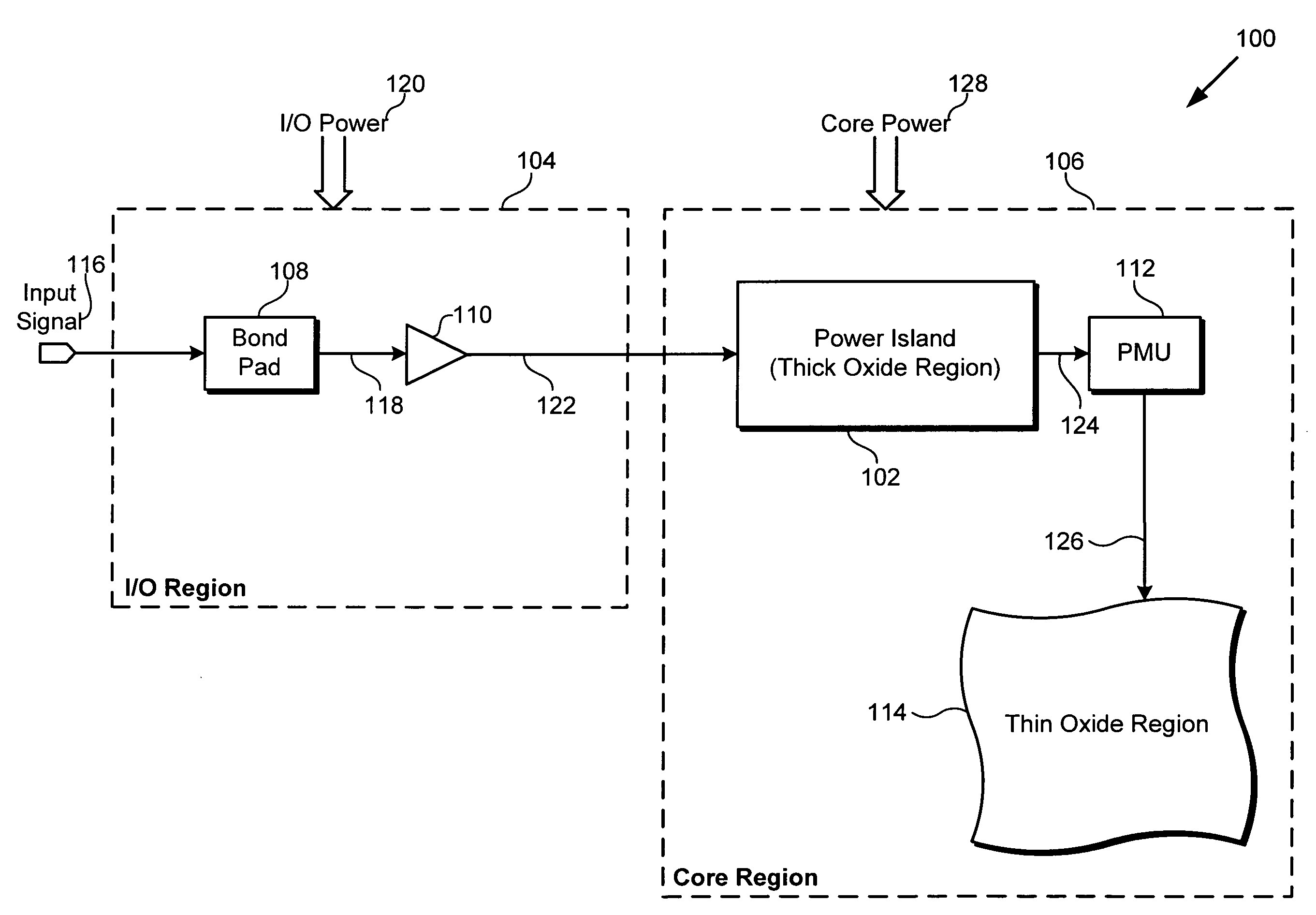
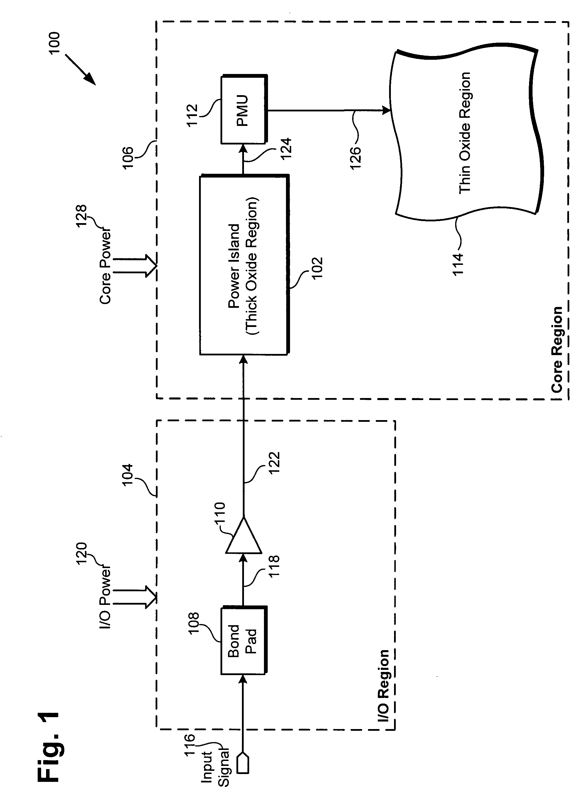
[0015]FIG. 1 shows a block diagram of conventional semiconductor die 100 with power management (also referred to hereinafter as “conventional power managing ...


PUM


Abstract

According to one exemplary embodiment, a power managing semiconductor die with reduced power consumption includes a power island including an event detection block and an event qualification block. The event detection block is configured to activate the event qualification block in response to an input signal initiated by an external event. The input signal is coupled to the event detection block, for example, via a bond pad situated in an I / O region of the power managing semiconductor die. The event qualification block is configured to determine if the external event is a valid external event. The event qualification block resides in a thin oxide region and the event detection block resides in a thick oxide region of the semiconductor die. The power managing semiconductor die further includes a power management unit configured to activate the event qualification block in response to power enable signal outputted by the event detection block.

Description

BACKGROUND OF THE INVENTION[0001]1. Field of the Invention[0002]The present invention is generally in the field of semiconductor dies and circuits. More particularly, the invention is in the field of power management in semiconductor dies.[0003]2. Background Art[0004]Semiconductor device leakage current (e.g. transistor leakage current) can cause an undesirable increase in power consumption in semiconductor dies utilized in electronic devices such as battery powered devices, which include wireless communication devices, such as cell phones, and wireless human interface devices, such as wireless keyboards, mice, and game controllers. In an effort to reduce leakage current, a power management technique can be utilized whereby a power island of a semiconductor die is used to turn on the remaining regions of the die, and to turn off those remaining regions whenever the battery powered device is idle.[0005]A conventional power island, which remains continuously activated (i.e. remains co...

Claims


Application Information

Patent Timeline
IPC IPC(8): H01L29/10
CPCH03K19/0016
Inventor LOU, WENKWEI
Owner AVAGO TECH INT SALES PTE LTD
Why Eureka
Eureka Blog
Learn More