

Semiconductor memory device and operation method of the same
a memory device and semiconductor technology, applied in the field of memory devices, can solve the problems of reducing system stability and system reliability, affecting system stability, and affecting system stability, and achieve the effect of sufficient operation margin for data access and stable operation
- Summary
- Abstract
- Description
- Claims
- Application Information
AI Technical Summary
Benefits of technology
Problems solved by technology
Method used
Image

Examples
Embodiment Construction
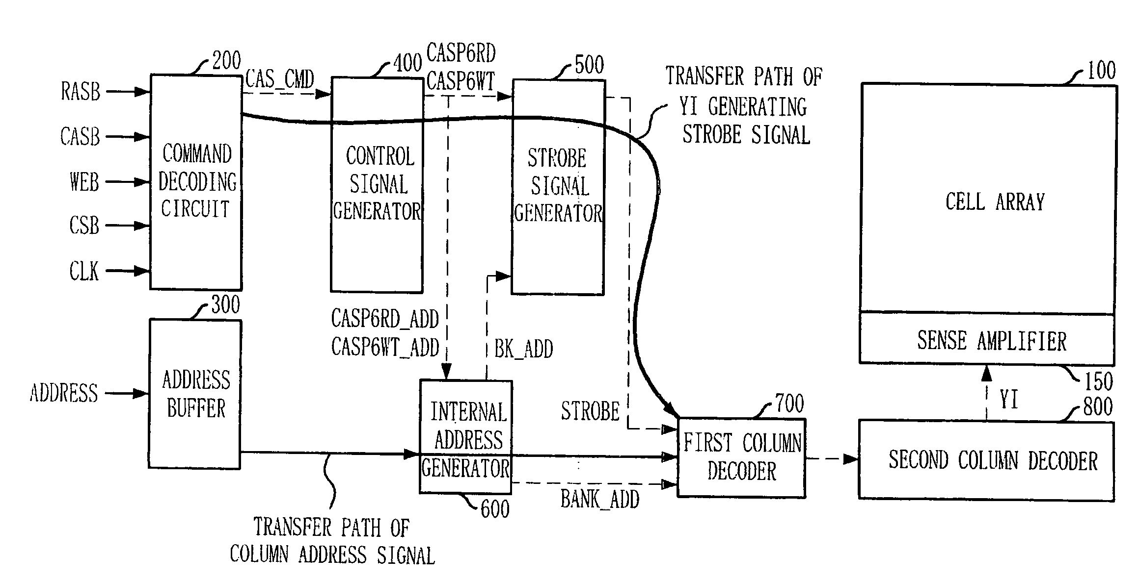
[0032]Hereinafter, a semiconductor memory device and an operation method of the same in accordance with the present invention will be described in detail with reference to the accompanying drawings.
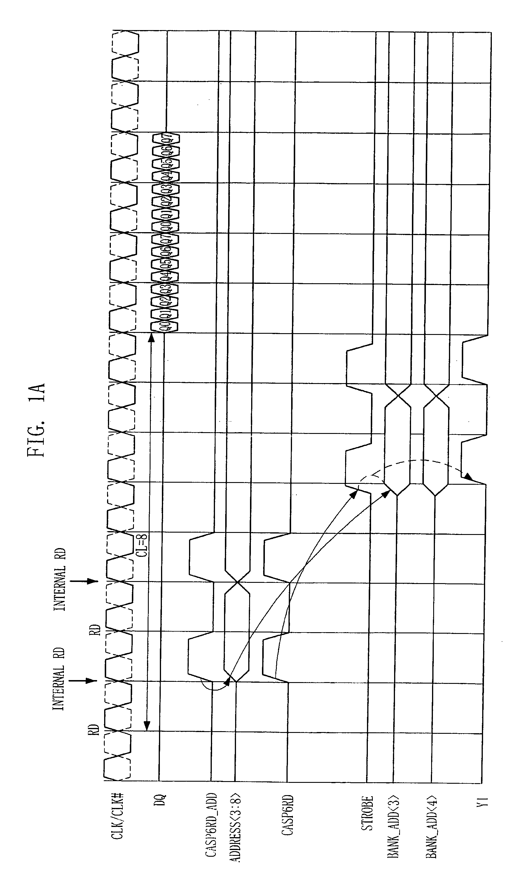
[0033]FIG. 2A is a timing diagram of a read operation performed by a semiconductor memory device in accordance with an embodiment of the present invention.
[0034]Referring to FIG. 2A, in a read mode, when a read command RD is received from outside, read address latch strobe signal CASP6RD_ADD is activated at a falling edge of a system clock, whereby a column address signal ADDRESS3:8> is generated. That is, contrary to the typical case, the column address signal ADDRESS3:8> is generated after 0.5 tCK from when the read command RD was applied and may have an effective window of a width of 2 tCK according to a minimum interval between commands. Meanwhile, a read column access signal CASP6RD, which serves as a source for a column selection signal YI, is generated after 1 tCK from when the rea...
PUM
 Abstract
Description
Claims
Application Information